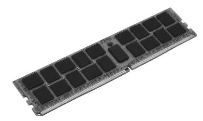
There is no question that the memory hierarchy in systems is being busted wide open and that new persistent memory technology that can be byte addressable like DRAM or block addressable like storage are going to radically change the architecture of machines and the software that runs on them. Picking what memory might go mainstream is another story.
It has been decades since IBM made its own DRAM, but the company still has a keen interest in doing research and development on core processing and storage technologies and in integrating new devices with its Power-based systems.
To that end, IBM Research is announcing that it has successfully created and tested phase change memory (PCM), an alternative storage that sits between DRAM and flash on the memory hierarchy much like the 3D XPoint memory developed by Intel and Micron Technology, that stores three bits per memory cell – an important development if the cost of PCM is to be brought down to be more competitive with DRAM and flash. IBM is also showing off a second generation of PCM memory cards that it has developed using existing PCM technology and coupled very tightly to its Power8 systems using its Coherent Accelerator Processor Interconnect (CAPI) interface.
Phase change memory has been in development since the 1970s, and is one of the many contenders as an adjunct to DRAM and flash in the memory hierarchy. As the name suggests, the ones and zeros in binary data storage are induced by a phase change in a material, in this case an alloy called chalcogenide that has a mix of antimony, germanium, and tellurium that with the application of heat can be induced into a crystalline or amorphous state, and data can be stored in either state which is extremely useful. Micron originally developed its first generation of PCM memory chips for smartphones because PCM is extremely fast and uses very little power compared to flash, but it is based on a complex substance and is difficult to manufacture. So driving up the bit density, and therefore the overall capacity, of PCM is an important step towards commercializing this technology. That said, given the relatively low storage density of PCM compared to flash and perhaps 3D XPoint, it stands to reason that PCM may be relegated to the parts of systems where latency of access, persistence of data, a high durability are more important than capacity. PCM can take up to 10 million write cycles, says IBM, compared to about 3,000 write cycles for the kind of flash used in a USB stick these days and falls even lower to maybe 300 to 500 cycles with triple level cell (TLC) flash that is commonly used in enterprise applications. Compared to this flash, PCM has what is effectively an eternal wear level.
In any event, up until now, PCM was able to store one bit per memory cell, but a team of researchers at IBM’s lab in Zurich, Switzerland have demonstrated they can store two bits per cell and a path to three bits per cell – equivalent to the density of modern flash memory. The PCM research is being led by Haris Pozidis, manager of non-volatile memory systems at IBM Research, and the team’s findings are being presented in a paper at the International Memory Workshop in Paris.
“Phase change memory is the first instantiation of a universal memory with properties of both DRAM and flash, thus answering one of the grand challenges of our industry,” Pozidis said with regard to the research that IBM has been doing. “Reaching three bits per cell is a significant milestone because at this density the cost of PCM will be significantly less than DRAM and closer to flash.”
This is, of course, precisely the part of the memory hierarchy that Intel and Micron are pursuing with their 3D XPoint memory, which many speculate is based on resistive RAM (ReRAM) technologies, not PCM. At this time, 3D XPoint is implemented using a 20 nanometer process and stores data at a density of one bit per cell (SLC) and a 7 microsecond latency for reads and delivers on the order of 78,500 IOPS in a 70/30 read/write mix that is typically used to characterize storage. (These stats are courtesy of Chris Mellor over at our sister publication, The Register.) DRAM access is on the order of 200 nanoseconds, or about 35X faster than Intel’s Optane 3D XPoint, but 3D XPoint is about four times faster on writes than a PCI-Express flash unit using the trimmed down NVM-Express protocol and about twelve times faster than this flash on reads.
To push the limits on PCM and push it up to MLC and then TLC densities, IBM created its own 2×2 Mcell array with a four-bank interleaved architecture and comprising a 64K cell array, and running it at elevated temperatures and with 1 million set and reset endurance cycles was able to show two bit per cell storage and a means of delivering three bits per cell. To accomplish this feat, IBM has come up with a set of metrics that can monitor the state of the PCM cells that are immune to the effects of the drift in the state of the underlying material and coding and detection methods that are tolerant of this drift and therefore prolong the longevity of the storage as its density is increased.
It is unclear how this research will be used to improve actual PCM devices, but IBM is always interested in licensing its technology.
In the meantime, Big Blue is showing off the second generation of PCM cards interfacing with its Power8 systems and delivering much better performance than is possible with flash storage.
Back in early 2014, IBM researchers partnered with Micron and FPGA maker Xilinx to create a PCM server card based on Micron’s P5Q PCM chips under Project Theseus. These 128 Mbit PCM chips are manufactured in very mature 90 nanometer techniques by Micron and cycle at 66 MHz. The P5Q chips have very asymmetric read and write performance, with writes taking about 1.15 milliseconds and reads taking about 75.25 microseconds, which translates into 860 operations per second on writes and 13,290 operations per second on reads. This first generation card married a Xilinx Zynq-7045 FPGA board (which was programmed as a memory controller) with two channels of PCM memory, which delivered 65,000 read IOPS at a latency of 35 microseconds and 15,000 write IOPS at a latency of 61 microseconds, and importantly for applications that require consistency of performance, 99.9 percent of the I/O requests were completed within 240 microseconds, which was 12X better than MLC flash devices and 275X better than TLC flash devices that IBM tested two years ago.
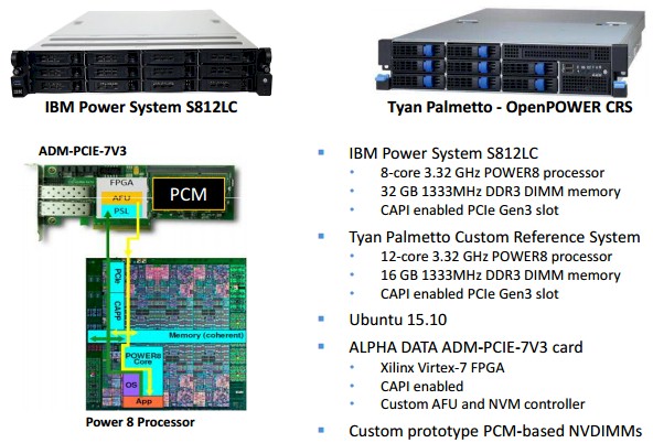
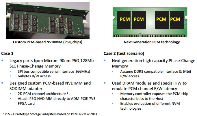
With its second generation PCM prototype, IBM was specifically interested in testing how to link PCM memory in a PCI-Express form factor would perform when linked to the Power8 processor complex using CAPI ports. This new card was implemented using the same P5Q PCM memory from Micron. IBM also tested a next generation PCM card that emualted PCM using DRAM and then put the memory on a DDR3 interface, which is scenario two in the chart below:
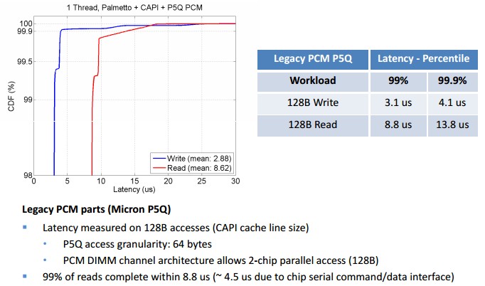
With the CAPI interface, the older P5Q PCM memory card was considerably faster than the original implementation that IBM did two years ago in its initial tests. As you can see, the performance is pretty high and also predictable:
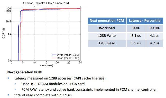
And with the improved PCI-Express card, which puts the emulated PCM memory on DIMMs that plugs them into the FPGA card, the latency drops even further and the gap closes a bit between reads and writes, too:
It will be interesting to see how actual PCM memory does compared to this emulated PCM memory. But with the emulated PCM, IBM says that it is working to squeeze more performance out of the CAPI-FPGA-PCM stack by optimizing its protocols and is looking to support multiple PCM channels on the cards (as it did with its initial experiments two years ago) to boost the throughput and capacity of the PCM memory. Now, when the next generation PCM is actually available, IBM and its partners will be ready to roll it into production.
It is unclear what IBM’s plans are with regard to 3D XPoint memory, but anything it is doing with PCM is can, in theory, do with 3D XPoint. While Intel is expected to emphasize its Optane SSD and DIMMs for its own Xeon systems, Micron can sell its portion of the 3D XPoint memory coming out of their joint operations to whomever it chooses. Micron has been mum on precisely what its plan is here, but it is likely that some OpenPower partners, such as Alpha Data who made the PCI-Express cards used in the CAPI tests above, could integrate any number of different memory technologies on their FPGA cards and create controllers to drive them and act as an interface to the Power8 compute complex through CAPI.




IBM main disadvantage here lies in that they have basically now zero FABs on their own. And in terms of memory only those companies with FABs basically supply and rule the market.
What is up with you and you need for chip Fab ownership, IBM still retains some research fab capacity, and do you not understand the economy of scale that the third party chip fabrication industry offers to all those who are fabless chip designers IBM(recently), Apple, AMD, Nvidia, third party OpenPower licensees, etc. All of of these fabless companies are using the third party chip fabrication industry, and that very same third party chip fabrication Industry is spreading the chip fabrication process node shrink R&D and physical plant expenses across an entire market of fabless chip designers!
What is it with you and your need for these fabless chip companies to have to posses anything chip fab related, but maybe some very limited in-house RESEARCH chip fab capacity! Full market volume chip fabrication capacity UNUSED is one very expense anchor around any company’s neck and that’s why IBM went fabless!
OranjeeGeneral do you have some excess codpiece space/capacity related ego issues that necessitates your need for any one chip development interest to posses its own very expensive chip fabrication physical plant holdings, because that chip fab capacity NOT continuously used to its fullest utilization level bleeds way too much cash for even the largest of companies!
That’s for logic which is a complete different field, there is zero non-fabs companies in memory today! Makes no sense as you said economy of scale dictates here margins in memory tend to be much smaller than for logic chips so you can’t compare these two at all. Just do a bit of research that’s all I am asking. IBM is just hyping up as usual it is the same with the Quantum computing stuff there are zero applications for it at the moment. Their TrueNorth neuro-chip not that hot either. IBM is desperate to get media attention and get their stock price going as their key market is faltering quickly. They have been over run by other hyperscales which push them out in their mainframe market and Softlayer itself isn’t going so hot in comparison simply because they stick with their in-house architecture which has serious problems to compete on price with Azure, Amazon or Google’s cloud
I am the only person thinking “database transaction log” for in-memory databases?