Ethernet switching has its own kinds of Moore’s Law barriers. The transition from 10 Gb/sec to 100 Gb/sec devices over the past decade has been anything but smooth, and a lot of compromises had to be made to even get to the interim – and unusual – 40 Gb/sec stepping stone towards the 100 Gb/sec devices that are ramping today in the datacenter.
While 10 Gb/sec Ethernet switching is fine for a certain class of enterprise applications that are not bandwidth hungry, for the hyperscalers and cloud builders, 100 Gb/sec is nowhere near enough bandwidth, and 200 Gb/sec, which is off in the hazy horizon of the Ethernet roadmap, is something that organizations might plan for deployment in maybe 2018 or 2019 or 2020. Well, how does 400 Gb/sec Ethernet sound? Will next year be soon enough? Delivering 400 Gb/sec switching next year is precisely what switch chip upstart Innovium plans, and you can bet its Teralynx chips have gotten the attention of the hyperscalers and cloud builders that will very likely be its very first customers.
Innovium was founded in 2015, and it is entering what would seem to be a crowded switch ASIC market. Broadcom is the leader in datacenter switching with its Trident, Tomahawk, and Dune chips, which are tuned for different speeds and workloads. Fellow upstarts like Barefoot Networks with its Tofino chip and Cavium with its XPliant chip are trying to carve out business against Cisco Systems, Juniper Networks, and Hewlett Packard Enterprise, who all still make some of their own ASICs for their own switches, and against niche players with expertise in HPC and hyperscale, including Mellanox Technologies with its Spectrum 100 Gb/sec Ethernet and Quantum 200 Gb/sec InfiniBand products and Intel with its 100 Gb/sec Omni-Path gear. Networking is a lot more interesting than it has been in years, just like compute. (That could be a happy coincidence, but it is probably more due to the fact that the hyperscalers are driving innovation with their dollars.)
The founders at Innovium have been in the switch chip business for a long time, and it is not a surprise that they have been able to raise $90 million in three rounds of venture funding, backed by Greylock Partners, Redline Capital, Walden International, Capricorn Investment Group, Qualcomm Ventures, and an undisclosed bunch of corporate investors that we think probably includes a few hyperscalers given the fact that Innovium is explicitly targeting the cloud and hyperscale market, which company co-founder and CEO Rajiv Khemani, tells The Next Platform he reckons is worth about $2 billion or so just for ASICs. (We will walk you through the math in a bit. Sit tight.)
Khemani ran Intel’s network processing business for a bunch of years and then was chief operating officer at Cavium for a decade before joining up with Puneet Agarwal, who is chief technology officer, and Mohammad Issa, who is vice president of engineering, to start Innovium and really push Ethernet to higher bandwidths. Agarwal was CTO for switching at Broadcom for a decade and holds more than 80 patents, and Issa was vice president of engineering at Broadcom for nine years, and they brought the Trident and Tomahawk chips off the drawing board and into most of the datacenter switches of the world (like something in excess of 90 percent market share). Khemani says that Innovium has more than 80 employees, and most of them are engineers working on the Teralynx chip and its successors out on its own roadmap.
“Everybody wants high bandwidth and low latency, especially at the top of rack where the switch is a single point of failure inside of a rack of servers,” explains Khemani. “If a top of rack goes down, that is 40 to 80 servers that are down, and that is a big pain point for them. So they want higher uptime, higher bandwidth, and lower latency as the traffic is traveling inside the datacenter and to customers. And the largest datacenters want lower energy and they want simplicity and automation so they can lower operational expenses.”
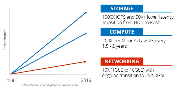
They also want to get networking back in synch – or at least better in synch – with the growth in compute and storage. They are out of whack, as this simplistic comparison shows, and the network is the bottleneck:
Even if you want to be generous, you could say the 100 Gb/sec transition is under way. But it is only really happening at the hyperscalers and some cloud builders and HPC centers, and even then, on the server is it really still one, two, or sometimes four 10 Gb/sec pipes coming out of the machine and often up to a 10 Gb/sec or 40 Gb/sec switch. Networking bandwidth has just not kept up with compute and storage capacity.
The most obvious question is how can Innovium get a 12.8 Tb/sec ASIC capable of driving a large number of 400 Gb/sec ports out the door when no one else seems to be moving all that fast towards that goal. The answer is simple. Or rather, simplicity and focus.
“We had to start with a clean sheet of paper,” says Khemani. “You cannot leverage all of the stuff that is aimed at enterprises and service providers. We understand the problems that these large datacenters have and we focused on innovation aimed at them. It is a very optimized solution, and we do not put features that, for example, are necessary for a campus network into Teralynx. This allows us to make a chip that provides better performance, takes less area, is easier to implement, easier to verify, and allows us to get to a volume production ramp quicker.”
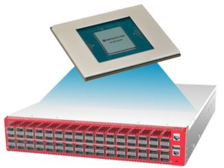
This is called the Teralynx 7, oddly enough, which would seem to imply that there have been six prior generations. Because of the minimalist design, the ASIC can pump out 12.8 Tb/sec of aggregate switching bandwidth, and it also has enough room for a 70 MB buffer. (The largest ones on the market, which are in the Dune family of chips from Broadcom, have 40 MB buffers, and this really helps with quality of service on heavily loaded networks.) Importantly, the Teralynx ASIC has a port-to-port latency hop of under 350 nanoseconds, and the full gamut of Ethernet switch ASICs ranges from a low of 400 nanoseconds to around 2 milliseconds, according to Khemani. That 350 nanoseconds latency for the Teralynx is nowhere near the 100 nanoseconds for the latest InfiniBand and Omni-Path switches, but it is low enough for the kinds of workloads used in hyperscale and clouds, where other latencies in the datacenter swamp those extra few hundred nanoseconds and make them seem not nearly as useful as a lower-cost, higher bandwidth device. HPC needs low latency more than it needs bandwidth in a lot of cases; clouds and hyperscale applications need high bandwidth with reasonable and consistent latency in a lot of cases.
The Teralynx 7 chip has flexible port configurations and can deliver a mix of ports running at 10 Gb/sec, 25 Gb/sec, 50 Gb/sec, 100 Gb/sec, 200 Gb/sec, and 400 Gb/sec all from the same device. The SERDES circuits driving these ports are flexible, meaning they can be configured to run at 10 Gb/sec or 25 Gb/sec signaling rates using NRZ encoding or run at an effective 50 Gb/sec using PAM-4 encoding (the clocks stay the same, but two bits can be transmitted per signal). The Teralynx chip has a maximum of 256 SERDES lanes, which can be configured as needed to drive those ports.
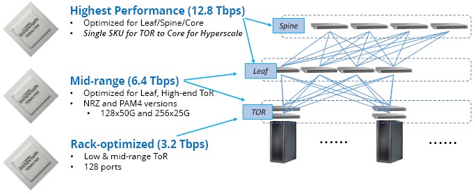
The Innovium ASIC will be implemented in a 16 nanometer process and there will be variants that have 3.2 Tb/sec and 6.4 Tb/sec switching capacities as well as the top end 12.8 Tb/sec capacity. That top end Teralynx chip will be able to drive 128 ports running at 100 Gb/sec, 64 ports running at 200 Gb/sec, or 32 ports running at 400 Gb/sec, and given that bandwidth, it is reasonable to expect someone will make modular aggregation switches using the 400 Gb/sec ports as well as use them as fat spines in leaf/spine networks. We do not know how many billions of packets per second the Teralynx can process, but presumably it is a lot.
Innovium did not go into too much detail, but the Teralynx chip has an embedded 1 GHz ARM CPU core for adding network functions and a set of network telemetry and analytics processing engines that Innovium calls Flashlight. It is this vast telemetry that allows for automated management of the network as the workloads are shifting around, and it is something that the hyperscalers and cloud builders have gone to great lengths to build in their network operations stacks. (Wouldn’t it be nice if it was just in the switch ASIC, where it belongs and where it can run at line speed?) The Teralynx chip also has a set of programmable forwarding plane functions that provide what Khemani calls “just enough programmability” so new and tweaked protocols can be added to the ASIC rather than having to wait for them to be implemented in a future generation of silicon. (This programmability is the key aspect of the Cavium XPliant and Barefoot Tofino chips that gives them an edge over other ASICs.) This Innoflex forwarding plane supports full Layer 2/3 forwarding as well as various tunneling protocols, including the MPLS that is popular with the hyperscale crowd.
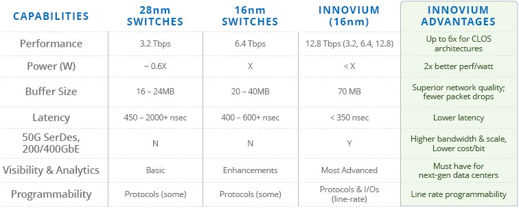
Here is how Innovium stacks the Teralynx up to the latest two generations of Ethernet switch chips, without naming names, of course:
Even as some switch ASICs in the 16 nanometer generation have been able to crank up the bandwidth and boost buffer sizes, they have also cranked up their power, in some cases they are north of 300 watts, on par with a GPU accelerator or an overclocked CPU. By stripping out all but the essential Ethernet features that hyperscalers and cloud builders want, Innovium has been able to quadruple the switching bandwidth compared to the 28 nanometer generations of ASICs while nearly tripling (in the worst case) the on-chip buffers while reducing the latency a bit and delivering about twice the performance per watt on a port running at 100 Gb/sec.
The big advantage in using a high bandwidth Teralynx ASIC in the kind of Clos networks that are popular at Google and at Facebook and at other hyperscalers is that it will take fewer switches to support a given number of ports. If you want to support 128 ports running at 100 Gb/sec and cross link them, using a 3.2 Tb/sec device would require four leafs and two spines using 6.4 Tb/sec switches and there would be three hops between any two servers not on the same top of rack switch. To do it with cheaper 3.2 Tb/sec switches would require eight leafs and four spines with the same number of hops. With the Teralynx, those 128 server ports would hang off the same top of rack switch – perhaps spanning as many as three racks, with some longer cables. The latency of connection between those multiple racks of servers would be much lower, obviously, because they would be talking within an ASIC, not hopping across multiple of them. A case in point is Facebook’s Backpack modular switch, which has 128 ports running at 100 Gb/sec and which was unveiled last November. (Bet Facebook wishes it had a Teralynx switch back then.)
The software development kit for the Teralynx ASIC is available now, and the chip will start sampling to early customers and partners in the middle to the end of the third quarter of this year, according to Khemani. As for the cadence of the Teralynx roadmap, Khemani says Innovium has shared it with some key early customers, but is not yet tipping his hat. What he will say is that the first product is the hardest one, and that most of the money it has raised through venture funding is still in the bank so it has plenty of cash to build out that roadmap.
“The design is very modular, so we can take building blocks and scale it up and down very easily,” he says. So, it would not be surprising to see a 10 nanometer switch with twice as many elements that can drive 25.6 Tb/sec and maybe, just maybe, 800 Gb/sec ports, and that will take twelve to eighteen months before standards are set and maybe two to three years before it is productized.
One last thing: We wanted to do the math on the total addressable market. So here goes. Depending on who you ask, the Ethernet switching market is around $30 billion, and the datacenter portion of that is around $11 billion to $12 billion of that. If you do a blended gross margin of somewhere between 55 percent to 60 percent for those datacenter switches, that gives you somewhere around $5 billion for the cost of the components going into those datacenter switches. The switching silicon represents somewhere between 30 percent and 40 percent of that, which brings you to somewhere between $1.5 billion and $2 billion for the ASICs. If you assume the datacenter switching market will continue to grow, perhaps to $15 billion by 2020, then even at the low end, this is still a $2 billion addressable market.
And with such high bandwidth and such high radix on the Teralynx device, Innovium will be able to charge a premium and still compete well.



Curious about the PCI-E host connectivity shown in the diagram. Do they plan to build switches with built in generic compute attached (similar to what Pluribus has done with some of their own kit)?
Definitely some interesting possibilities there, if there are enough PCI-E lanes to do something meaningful.
PCIe 3.x prevents this from doing anything useful — all lanes at theoretical maximum don’t provide enough bandwidth, and 4.0 “only” doubles that. I.e., PCIe *is* the problem, despite all its conveniences. Or to look at it differently, the above 400Gbps should BE the “bus” between highly dense compute nodes. Abandoning the conveniences of PCIe is impractical, so rethinking the current-era gigantic/wasteful “half-height” compute blades should be the next step.
Let the race for massively parallelized micro-blades commence! (Since we can “duct-tape” 18+ Xeon-D NUCs into a 2U server rack slot w/82599 each, getting at least that many w/400Gbps NICs and PCIe 4.0 micro-buses seems achievable…)
–intensify security .at. g. m. to engage in further jolly banter