To keep their niche in computing, field programmable gate arrays not only need to stay on the cutting edge of chip manufacturing processes. They also have to include the most advanced networking to balance out that compute, rivalling that which the makers of switch ASICs provide in their chips.
By comparison, CPUs have it easy. They don’t have the serializer/deserializer (SerDes) circuits that switch chips have as the foundation of their switch fabric. Rather, they might have a couple of integrated Ethernet network interface controllers embedded on the die, maybe running at 1 Gb/sec or 10 Gb/sec, and they offload any more complex networking needs to devices that hang off the PCI-Express bus.
At the OFC 2018 optical networking and communication conference this week, FPGA maker Xilinx is showing off two things that advance networking on its Virtex UltraSscale+ line of FPGAs. The first is that it has goosed the speeds of the SerDes on the Virtex UltraScale+ devices, specifically by moving to pulsed amplitude modulation, like the key Ethernet switch ASIC vendors are doing to boost the performance of their SerDes and therefore the pipes coming into and going out of their switches. Mellanox Technologies was first out of the gate last summer when it unveiled PAM-4 encoding with its Spectrum-2 Ethernet ASICs, which will push port speeds up to 200 Gb/sec speeds with a plan to reach 400 Gb/sec. Broadcom followed up in January of this year with PAM-4 support in the “Tomahawk-3” Ethernet ASICs.
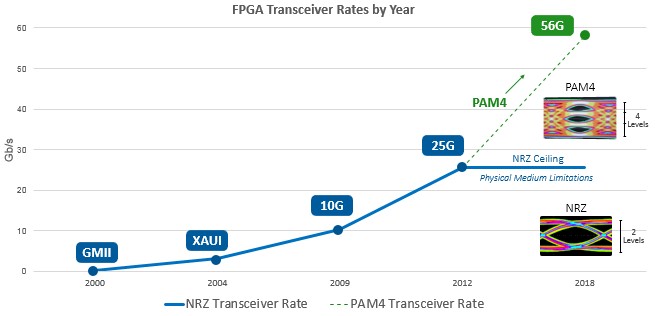
The jump to PAM-4 encoding is necessary and the non-return to zero, or NRZ, modulation used with prior generations of Ethernet switching hardware, cabling, and server adapters is not cutting it. NRZ can encode one bit on a signal, but with PAM, multiple levels of signaling can be encoded and therefore multiple bits can be packed into the signal. With PAM-4, there are four levels of signaling, which allows two bits of data to be encoded at the same time on the signal; this doubles the effective bandwidth of a signal without increasing the clock rate of that signal, thereby saving heat. It is possible with PAM to cram even more bits on a wire, and in theory you can do three bits per signal with PAM-8 encoding and four bits per signal with PAM-16 encoding. The combination of faster lanes and denser encoding is how the networking world is going to ram up networking bandwidth in the years ahead. It is looking like a real challenge to get SerDes to run at anything higher than 100 Gb/sec. (That number is after the signal encoding and forward error correction overhead is taken off.)
In many cases, where companies are creating their own prototype switches (in some cases they are secretive networking vendors, in others they are secretive hyperscalers and cloud builders), they build them first in FPGAs and then, if it makes sense, they cut an ASIC. In other cases, these network-juiced FPGAs sit alongside a switch ASIC, performing selected functions in front of the switch ASIC, so having lots of native high speed ports is a necessity.
Back in the day, Xilinx used to just OEM its SerDes from networking providers in the industry and block them into its FPGA designs, but for the past several generations it has designed its own SerDes because it wants to move at its own pace and because there are subtle differences required between hard-etched switch ASICs – application specific integrated circuits – or ASSPs – that’s application specific standard parts – and malleable FPGA compute.
“The SerDes are similar at a very high level, in that they solve the same problems and they talk to the same optics and use the same protocols, and they work over the backplanes in similar ways,” Mike Wissolik, senior product line manager for high end FPGAs at Xilinx, tells The Next Platform. “Our SerDes are a little different in that they are not purpose built for a specific standard. Often, on ASSPs and ASICs, a port might be defined as having four lanes running at 25 Gb/sec, and vendors just have a 25 Gb/sec SerDes that is purpose built to do that. With FPGAs, because it is a reprogrammable device, we have to be able to do signaling ay 10 Gb/sec, 25 Gb/sec, or 50 Gb/sec on any port at any time, and this is really our value proposition just like flexible compute is. This is about future proofing. If new protocols emerge, the ASICs and ASSPs have to do a tape out, but with FPGAs, you tweak the IP and you are good to go.”
Here is where the new 56 Gb/sec signaling on the SerDes (which gears down to 50 Gb/sec after encoding overhead) fits into the Virtex UltraScale+ lineup at Xilinx:
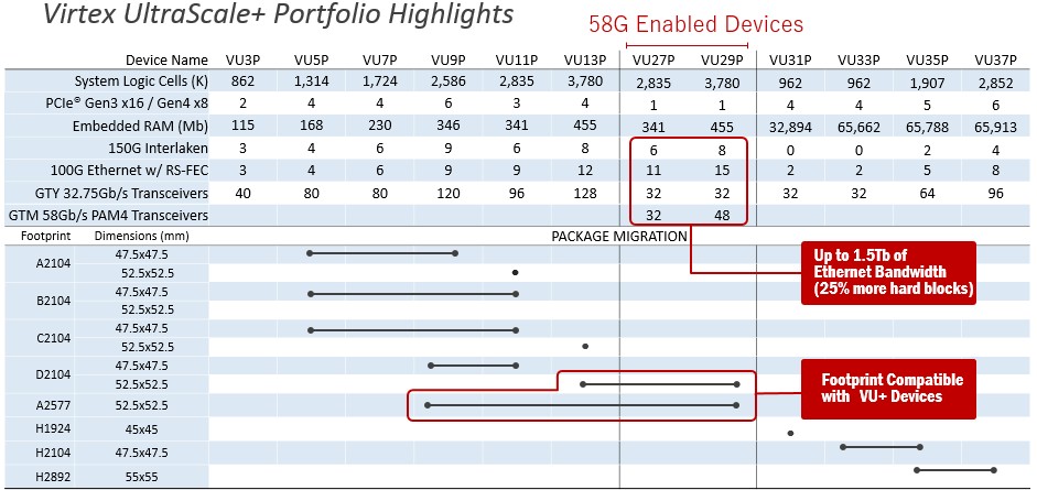
Basically, Xilinx is taking the 25 Gb/sec SerDes in the VU11P and VU13P devices and replacing it with the shiny new 58 Gb/sec SerDes to make the VU27P and VU29P. The SerDes can talk whatever protocol you want: InfiniBand, Ethernet, or even some of the custom protocols that the hyperscalers have created for their machine learning clusters. These updated Virtex UltraScale+ FPGAs, which are made using the 16 nanometer FinFET processes from Taiwan Semiconductor Manufacturing Corp, will roll out later this year.
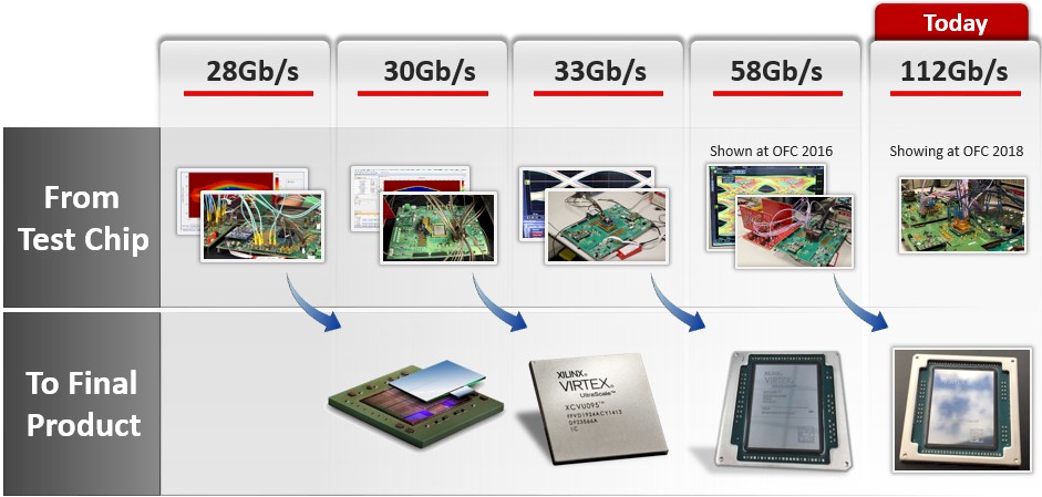
Looking out into the future, Xilinx is demonstrating a prototype SerDes that can do 112 Gb/sec signaling, doubling up the bandwidth again. This technology demonstration is several years ahead of production, but gives Xilinx customers in the datacenter and communications businesses time to provide feedback on what they need in future devices. At this speed and with PAM-4 modulation, a single lane on the SerDes will be able to run at 100 Gb/sec. This test chip, which is being shown at OFC 2018, is etched using future 7 nanometer processes from TSMC and is therefore a few years down the road to production. Based on past trends, sometime around two years from now there will be announcements for deliveries maybe later in 2020. Beyond that, it is hard to say what will happen, because many in the industry think that getting past 100 Gb/sec on a SerDes lane is going to be very tough indeed.




Be the first to comment