It has happened time and time again in computing in the past three decades in the datacenter: A device scales up its capacity – be it compute, storage, or networking – as high as it can go, and then it has to go parallel and scale out.
The NVLink interconnect that Nvidia created to lash together its “Pascal” and “Volta” GPU accelerators into a kind of giant virtual GPU were the first phase of this scale out for Tesla compute. But with only six NVLink ports on a Volta SXM2 device, there is a limit to how many Teslas can be linked together. In the hybrid cube mesh used in the DGX-1 servers from Nvidia, that limit is eight GPUs in a single node, and the system also has to rely on much slower PCI-Express switches to link a complex of GPUs together with the pair of Xeon CPUs inside a server node because the Xeon processors do not support the 25 Gb/sec signaling required to create an NVLink port. (IBM’s Power8+ and Power9 processors do have native NVLink ports, and the GPU complex can be directly linked to the CPU complex, which is a big plus when you want to have memory coherency across the CPU and GPU memories.)
So Nvidia has moved outside of its comfort zone and further into the world of networking to create its own NVLink switch, appropriately enough called NVSwitch, which was unveiled at the GPU Technology Conference in the company’s home stomping grounds of San Jose.
Unlike some of the switches that we see in the HPC arena coming out of China, which are derivatives of InfiniBand switching that are licensed from Mellanox Technologies, the NVSwitch ASIC is a homegrown device that has been under development for the past two years, Ian Buck, vice president and general manager of accelerated computing at Nvidia, tells The Next Platform. The NVSwitch ASIC has over 2 billion transistors, about a tenth of the Volta GPU, and it creates a fully connected, non-blocking crossbar switch using the NVLink protocol, which means every port on the GPUs linked to the switch can talk to all of the other ports (in a point to point manner) at full speed.
The switch chip has a total of 18 ports, which provide 50 GB/sec of bandwidth per port and which, if you do the math, use 25 Gb/sec signaling just like the NVLink ports on the Volta GPU accelerators and the IBM Power9 chips. The NVSwitch has an aggregate of 900 GB/sec of switching bandwidth, and a bunch of the switches can be interconnected and cascades to scale the Tesla network in any number of topologies. The ports on the switch aggregate eight lanes of 25 Gb/sec signaling
“We spared no expense on this, and we wanted to make sure that we were never limited by GPU to GPU communication,” says Buck.
In his keynote address at the opening of the conference, Nvidia co-founder and chief executive officer Jensen Huang said that the NVSwitch came out of work done by chief technology officer Bill Dally, the Stanford University professor who literally wrote the book on networking, and that the effort was the result of hundreds of millions of dollars in investment on the part of the company. (That investment figure also included some of the engineering that went into the DGX-2 systems that Nvidia is initially using the switch in, which we will cover in detail separately.)
The important thing is that at 50 GB/sec, a NVSwitch port has 3.1X the peak bandwidth of a PCI-Express 3.0 x16 slot, which provides 16 GB/sec, that is common on a server today. This 16 GB/sec also represents the top bandwidth of a PCI-Express switch port, which is important because many system designs that include NVLink to hook together the GPU compute nonetheless have to rely on PCI-Express switches to attach the CPU complex to the GPU complex. This hierarchy of networks presents some challenges, but with the NVSwitch, the GPU complex will be more scalable and be able to run AI models faster, or run larger models with many more layers, as the GPU compute is scaled within a node.
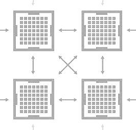
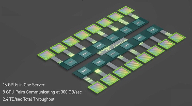
The NVSwitch will also presumably be very interesting to the HPC crowd, and interestingly could be used to sit between processors like IBM’s Power9 and various Volta Tesla accelerator GPU complexes. The important thing is that the NVSwitch is purpose built to speak the memory semantics of the GPUs and to use every bit of its bandwidth towards that end and not to support other protocols like InfiniBand or Ethernet. It is, for all intents and purposes, a memory switch, with direct GPU-to-GPU links scaling up as high as 300 GB/sec when all six NVLink ports on each Volta are banded together to create a fat pipe, like this:
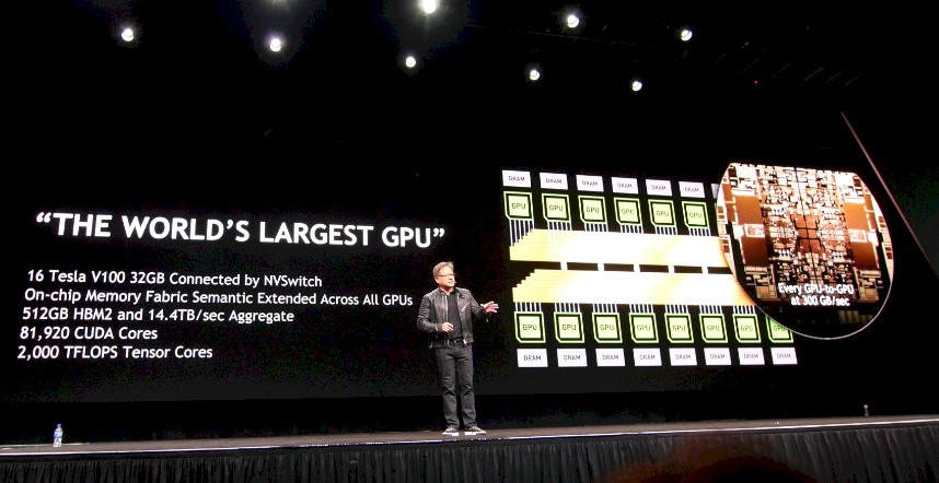
That is a whole lot of bandwidth to have between the eight GPUs on each side of the crossbar in the NVSwitch. We are not sure how many hops it takes to get to the other side or how much bandwidth there is, but it takes six of the switch ASICs to link eight of the GPUs together, and then the two complexes of eight GPUs are connected with the remaining ports. That is a total of 96 downlink ports to link the GPUs from the dozen NVSwitch ASICs that comprise the interconnect fabric and another 120 ports to link the two sides of the network to each other, for a ratio of an aggregate of 4.8 TB/sec of bandwidth into the switch from the GPUs to 6 TB/sec of bandwidth linking the two halves of the network to each other.
What the NVSwitch does as Nvidia is currently using it is create a big, monstrous virtual GPU that has sixteen Volta Tesla V100 accelerators linked by that memory fabric into a distributed compute unit that has 512 GB of HBM2 frame buffer memory for models to run around in, with a total of 81.920 cores and 2 petaflops of aggregate compute using the FP16 half precision Tensor Core units.
At the moment, Nvidia is not saying if it will sell the NVSwitch to OEM and hyperscale partners and for now it is only available in the DGX-2 systems. But given that Nvidia knows customers buy their systems from other suppliers or have them custom built by the ODMs to their own specifications, it stands to reason that NVSwitch will eventually be available as a standalone product. There are many other possible configurations of switch topologies that are possible and we will be exploring them in a future article. There are also ways that NVSwitch could be used for massive visualization or database acceleration workloads, too. This is by far the most interesting thing to come out of GTC 2018 yet.


“The important thing is that at 50 GB/sec, a NVSwitch port has 3.1X the peak bandwidth of a PCI-Express 3.0 x16 slot, which provides 16 GB/sec”
What? Counting bidirectional for NVlink but only unidirectional for PCIe? Why?
NVLink: 8 bits, 25 Gbps, Bidir, 8 bits/byte = 8x25x2/8 = 50 GB/s
PCIe Gen3: 16 bits, 8 Gbps, Bidir, 8 bits/byte = 16x8x2/8 = 32 GB/b
Nvlink port 3.1x faster than Gen3 PCIe? Not even close. Try 56% faster.
Standard Gen4 PCIe is 64 GB/s
PCIe Gen4 ESM25 is 100 GB/s
PCIe Gen5 will be 128 GB/s
It gets confusing to play with width and speeds together. You want to look at uni-directional line rate. PCIe Gen3 = 8 GT/s , NVLink = 25 GT/s , which is in-fact 3.2 times faster.
That translates into real bandwidth test results as well, that we’ve run at Rackspace internally.
Our tests indicate that PCie Gen3 is a horrible bottleneck today for scaling DL applications via 2 reasons:
1. Server to Server networking (Still 100Gbps NICs for x16 PCIe G3)
2. CPU-GPU Data movement ( Still 8T/s per lane, 1 direction)
We are trying to solve both via our Power9 server : Barreleye G2 (Supporting NVLink 2.0 and PCIeGen4)
Why you should take our observations seriously ? We don’t sell servers . We sell services on the hardware that’s tailor made for our customers and hence we don’t have vendor / protocol / architecture bias.
Very nice stuff.
Also, I hear that the giant new 51820 core GPU thus enabled can simulate playing Crysis at greater than one hundred frames per second.
Can someone please answer the following questions for me?
1) How close does PCIe 4 get to NVLink speeds?
2) When is it available on Intel partner nodes?
3) What is the performance difference between memory-to-CPU (no GPU involved) vs memory-to-CPU-to-GPU? I am under the impression that for larger data movement use cases, that NVLink and PCIe are much slower moving data from CPU memory into and out of GPU. Can someone please quantify this difference?