
Barefoot Networks is on a mission, and it is a simple one: To give datacenter switches the same kind of openness and programmability that X86 servers have enjoyed for decades in the datacenter.
With the Tofino 2 Ethernet switch ASICs that the company has just revealed, the company will be able to capitalize on the growing popularity of programmable switching in general and in the P4 networking programming language it created and shepherds in the open source community along with Google, in particular and to demonstrate that its chip designers can keep up with the fixed function switch ASIC makers when it comes to throughput, bandwidth, cost, power, and switch radix.
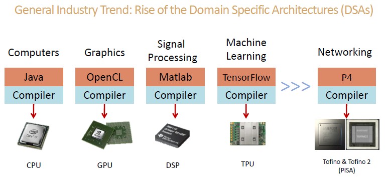
The inevitable drive to programmable switches in the datacenter mirrors the changes that have affected the major facets of compute in the datacenter, it is just finally time for this to come to switching, as Barefoot Networks chief scientist and co-founder Nick McKeown talked once again about with this handy chart:
“The bigger trend is that the cloud providers and hyperscalers in particular are producing a lot of silicon,” McKeown tells The Next Platform. “If anything, this trend has picked up over the last few years, and the silicon is no longer made just by the by the traditional chip vendors. The cloud and hyperscale companies are pushing it, and the trend is towards more domain specific architectures. The GPU is clearly being used everywhere, not just for graphics but also for machine learning, and the TPU and various other AI and machine learning chips, similarly are programmable devices with an instruction set fitting the domain and then a high-level language and a compiler for the specific type of solution.”
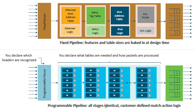
There is a big difference between a fixed function switch ASIC and a fully programmable one when it comes to packet processing, and this chart pretty well encapsulates it:
While this is all intellectually interesting, what really matters is that programmability doesn’t come at a high cost in terms of power, performance, or cost. That would be a non-starter for the high-end datacenters that would be early adopters of this technology because, frankly, only they have the skills and the intense need to have more programmable networks. (The rest of the IT environment will just get the benefits as they trickle down from on high, as with every technology.)
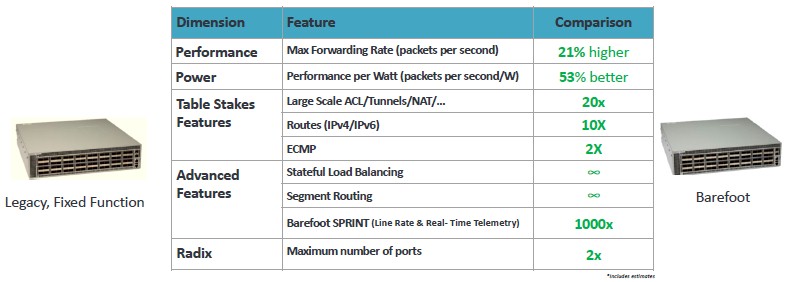
Ultimately, what matters – and what drove the chip designs and software stacks created by Barefoot Networks – is that a programmable switch meet or beat a fixed function one. Here is how Barefoot Networks stacks up its first generation Tofino 1 chip against an unidentified fixed function chip from merchant silicon vendor, which we suspect is the “Tomahawk 2” StrataXGS from Broadcom:
With the hyperscalers and cloud builders creating their own chips, and companies like Nvidia, Xilinx, and the Altera division of Intel figuring out how to deploy their respective GPU and FPGA architectures across a wider and wider variety of compute tasks – with ever-more programmable environments – it is reasonable to ask why they don’t.
“They are not going to be able to do better than we can because we are doing this all the time with a large team, and switching is definitely harder building a programmable network interface card as some of them have done or had done for them,” says McKeown. “It’s very, very hard for any of them either from the economics and the size of the team that they have to justify doing this and, frankly, they needed dump programmable network functions into the SmartNIC because nobody was doing it for them. We got there early enough with the switch chip and it really means there was no point in them doing it. Think about how these companies really differentiate from each other: They write different software. And so with our customers, we see a big variety in how they are using Tofino. In the past, with fixed function silicon from Broadcom, Marvell, and so on you could not do that. Everybody had to build the same product. If you look at the profiles the features in the Arista and Cisco switches using Tofino, they are different and that’s how it supposed to be. That’s exactly what we were trying to create. And for the cloud providers that are using Tofino, whether they’re in China or in the United States, their networks actually operate in different ways and they do that by programming them in different ways.”
Sticking With The Program
We profiled Barefoot Networks back in June 2016, when its first generation Tofino switch ASICs were announced alongside the P4 Studio programming tools first debuted after three years of development, pointing out that the last bastion of proprietary walls in the datacenter were starting to come down and that all of the other switch ASIC makers would have to react. And they have, particularly as the hyperscalers and cloud builders started to take a shining to having truly open switching, not just merchant silicon with an open network operating system, but an underlying ASIC for the control plane and data plane that was itself programmable. The Tofino chips have been used, among other things, to offload some of the processing in machine learning clusters to make the process faster and more efficient. Seeing the handwriting on the datacenter walls – it is scribbled on the top of rack and end of row switches – Arista Networks, which likes to be on the front end of any switching wave, adopted Tofino for some of its switches, and Cisco Systems, which prides itself on making its own ASICs, also quietly put them inside of its Nexus 3400 machines.
This set the stage with much wider adoption, which we anticipate will accelerate in 2019 and further in 2020, for programmable switches. And we think this time it won’t take switch makers two years to come around. Because some OEMs and a few ODMs have already built switches based on Tofino 1, adding Tofino 2 will be a relative snap.
With the Tofino 2 chips, Barefoot Networks is moving to 50 Gb/sec signaling and PAM-4 encoding to double-pump the bandwidth on the SERDES circuits, so they support an aggregate of 12.8 Tb/sec of bandwidth across the chip, which is twice as much as the Tofino 1 chip could do. The Tofino 1 was implemented in 16 nanometer technologies, and like almost every other chip designer pushing the process envelope, Barefoot Networks chose Taiwan Semiconductor Manufacturing Corp as its foundry. It has gone back to TSMC again for the Tofino 2, which is not a chip, strictly speaking, but a composite of multiple chips etched in different processes that are suited to the task.
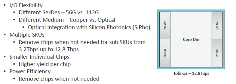
This multi-process chiplet strategy is also being used by AMD for its “Rome” Epyc server processors and by Xilinx for its “Everest” Versal FPGAs. This is the wave of the future for chips, and it is a good thing even if it does complicate manufacturing a little because smaller chips have higher yields than larger ones and older processes have higher yields than newer ones, too. Moreover, certain circuits – such as memory controllers and I/O controllers and communications controllers – actually perform worse when you shrink them too far, so etching them with larger transistors than is done with, say, core compute elements that do data processing on a CPU or FPGA or packet processing on a switch ASIC, is good for the overall design. With the Rome Epycs, the core I/O and memory controllers are on a central chip etched in 14 nanometers whole the cores are in chiplets that surround this core and are etched in 7 nanometers, which allows them to perform better.
Barefoot Networks is being a little cagey about what processes it is using to etch the Tofino 2, but confirms that the core die in the center of the chip package uses 7 nanometer processes, and the I/O tiles that implement the 50 Gb/sec signaling that wrap around them are etched with a prior TSMC process – our guess is the interim 12 nanometer process that Nvidia used to create the “Volta” GPUs.
This modular architecture is not just about making different parts of what would otherwise be a monolithic chip in different processes; it is literally about making it modular in the sense that you can mix and match, and add and subtract, components of the socket to make different products at different price points. So, for instance, while the SerDes are running at 56 Gb/sec, yielding 50 Gb/sec per lane after forward error correction and encoding, there is a way to snap in SerDes that run at 112 Gb/sec raw, yielding 100 Gb/sec per lane usable, at some point in the future when these faster SerDes are available – you will have to wait about two years for that, we think – without changing the packet switching cores. The chip package can be tweaked to drive copper or optical transceivers, and even snap in silicon photonics at some point in the future, Ed Doe, vice president of product, business, and strategy, tells The Next Platform. Lower bin ASICs can be created by taking a partially dudded packet switch core and only putting one, or two, or three SerDes block on the package, too. This allows Barefoot Networks to create a more diverse chip line with Tofino 2 than it had with Tofino 1, and that is precisely what it is going to do.
The top-end 12.8 Tb/sec Tofino 2 chip will support three different modes: 32 ports running at 400 Gb/sec, 128 ports running at 100 Gb/sec, and 256 ports that run at 50 Gb/sec but can be geared down to speak slower 25 Gb/sec or 10 Gb/sec speeds if necessary. (The Tofino 2 has about 50 percent better performance per watt than the Tofino 1, but the way.) In addition to the top bin 12.8 Tb/sec part, there will be one variant that has 8 Tb/sec of switching bandwidth, and another one that runs at 6.4 Tb/sec, essentially the same as the Tofino 1 but presumably able to drive half as many 50 Gb/sec, 100 Gb/sec, and 400 Gb/sec ports than the full-on ASIC package. The Tofino 1 chips were available in many different configurations, too, supporting 1.9 Tb/sec, 2.5 Gb/sec, and 3.3 Tb/sec, and 6.5 Tb/sec.
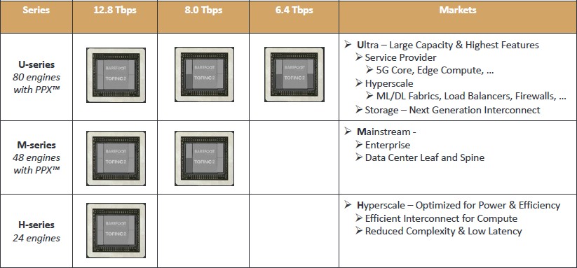
Not only will the Tofino 2 line be split up based on bandwidth, but on the number of packet processing engines (PPEs) that are activated on the packet forwarding cores. The Tofino chips had a static 48 PPEs, but the Tofino 2 will come with 24, 48, or 80 engines, depending on the series, plus another variant that is tweaked to be a network function accelerator. Like this:
So you can intermix the bandwidth and the number of engines, and therefore the price band, of the Tofino 2 chip you want in the switch. The H series, which is aimed at the hyperscalers, has only 24 engines but has the full 12.8 Tb/sec of aggregate switching bandwidth and the lowest latency and the cheapest price. The M series, aimed at the mainstream enterprise market top of rack switch and leaf/spine networks in large datacenters, comes with 8 Tb/sec or 12.8 Tb/sec of bandwidth and 48 engines like the Tofino 1. The U series is the high-end product, with the full 80 engines but coming with the full spectrum of bandwidth options. This one is aimed at service providers doing 5G networks, edge computing, and such as well as hyperscalers that want to embed all kinds of software functions such as load balancers and firewalls in the switch; it is also aimed at clustered storage, which needs bandwidth as well as some compute to offload algorithms to the switch. Barefoot Networks is just knocking off SerDes blocks to adjust the bandwidth. The Tofino 2 Advanced series, not shown on this chart, runs at 6.4 Tb/sec (meaning it has two of the four SerDes tiles on the chip) is aimed at NVF offload, compute offload, and network appliance applications.
This offload is important. McKeown says that one of the hyperscalers in China can replace the load balancing jobs that ran on 200 X86 servers simply by pulling the load balancer, written in P4, onto the Tofino chip and running it at line speed in the switch itself. But it doesn’t have to stop there.
“I tend to think of it as the following: The network consists of the software stack on the server, and then the network interface card, and the top of rack switch and up through multiple switch layers, then the network interface and the server software stack at the other end of the link,” McKeown explains. “There is this whole pipeline, and ideally the behavior of that entire pipeline is specified the same way using the P4 language. And if you are using P4 all the way along that pipeline, then you can choose and partition where those functions and features belong based on where they fit best, where they are most efficient, where they solve the problem best, and where you frankly what you have the hardware resources to support it.”
You tell us where the line between server and switch is in that world.
The other big theme, and what a programmable chip like the Tofino family offers, is what Barefoot Networks calls computational networking – something that happens in InfiniBand switches from Mellanox Technologies for HPC and AI workloads and that Barefoot Networks has also done, in its programmable way, by essentially running the parameter server in a machine learning cluster on the switch itself, implemented in P4.
“I think this computational networking is just getting started,” McKeown declares. “We have this very common experience when we are talking to customers who are thinking of programming the switch and their jaws drop when they realize the amount of computation they can do in the network as a consequence of Tofino. So they just do things that they have always wanted to do but they haven’t been able to do in fixed function silicon before. Not just the machine learning example, but a key/value store where you have got a large number of servers that sit behind the switch and you are caching very, very hot items on the switch. This works actually quite well with Memcached because it was very, very small and the hot elements get accessed a huge amount of the time, and so a relatively small amount of storage on the switch can give you not only a massive increase in performance, but it really reduces the tail latencies because you can cache the hot items that would normally lead to long access times. People initially think this is too good to be true, and ask us where’s the catch. And then over time they realize there isn’t a catch because you are doing all the processing at line rate. Any program that compiles and runs on the Tofino family will always run at line rate. There is no other choice because it is a feed forward architecture. And as a consequence, you never have to think about tuning the performance. It just will always run full speed. So for people doing computational networking, it is very easy because it is naturally real-time, and you don’t have to worry about interrupts and things like this.”
At some point, Broadcom or Cisco or Mellanox may take a run at Barefoot Networks. That is what that sounds like. Or AMD or Intel. Servers are going to be replaced by switches, and big blocks of memory and FPGA accelerators will be added to switches, and even more servers will go bye-bye. Maybe Intel should have bought Barefoot Networks instead of the interconnect businesses of QLogic and Cray? It’s not too late for AMD to jump in.
In any event, the Tofino 2 chips will be sampling in the first half of 2019, and should appear in products from OEMs and ODMs within about nine months and probably will be in use at the hyperscalers and cloud builders before that.


Just wait until someone applies deep learning to Ethernet packet switching. What might happen then?