For the past decade, we have documented the attempted rise of ARM processors in the datacenter, specifically in general purpose servers. It has been a decade of both hope and disappointment. But the datacenter is changing, with compute, storage, and networking being necessarily pushed to the edge of the network, closer to end users, because of the low latency demands of many modern applications and the great cost of moving and storing data centrally that may only be of temporary use. So the chance for Arm today is perhaps better than its prospects were a decade ago when this journey began.
Arm Holdings, the division of the Softbank conglomerate that owns the Arm architecture and licenses it to myriad chip developers for all manner of devices, already has dominant market share in smartphones, decent share in tablets, and the largest share among all chip makers (including Intel’s X86) of various kinds of auxiliary computing devices in the datacenter and out on the edge, such as in the 4G cellular network.
With the advent of 5G networking, the datacenter is going to get a lot edgier because 5G will eventually offer the kinds of bandwidths and latencies that only fiber wired networks could deliver. But in the short term, 5G bandwidth increases are still going to be pretty dramatic, with peak download speeds of 20 Gb/sec possible, compared to a peak of 1 Gb/sec with 4G; upload speeds are typically half the download rates, in theory. The actual performance of the 5G network will depend on which part of the spectrum is used in the cellular radio network and the terrain (including buildings) that the cellular devices are operating in. The point is, a factor of 20X boost in network performance, with anywhere from a factor of 60X to 120X reduction in latencies, is going to dramatically change the way the world uses cellular networks.
There is no question that cellular operators and those who create applications for these devices are going to use that bandwidth, and they are going to need sufficient networking, storage, and compute in 5G base stations and various edge locations that front-end the traditional wired telco points of presence (eventually the network has to talk over wires somewhere) or provide caching services to accelerate applications. If the network is fast in its own right, caching will become less necessary is the thinking, and instead of just delivering data, the network will be able to compute and act on it.
Knowing that this wave is coming, Arm late last year divulged its Neoverse architecture to better meet the needs of the datacenter and the edge when it comes to compute. Arm’s licensees have struggled to make meaningful sales of their processors in the datacenter. There are definitely proofs of concept with Marvell’s ThunderX2, there is hope for Ampere (which bought the X-Gene chips from Applied Micro), and Amazon seems to be pretty serious about its homegrown “Graviton” Arm server chips even if AMD, Qualcomm, and Broadcom dropped out, Calxeda is long kaput, and Samsung stopped before it really got started. At the edge, however, the Arm collective faces intense competition from Intel and now AMD with their respective Xeon and Epyc platforms, but Arm is the established player and they are the upstarts.
In this way, the “Helios” Neoverse E1 processor, which is aimed at the edge and which is a hot topic at this week’s Mobile World Congress (it’s now just called MWC, which is silly) in Barcelona, is perhaps more important for Arm’s aspirations in server compute than the “Ares” Neoverse N1 processors that were announced a week ago. To be perfectly clear, there will be edge variants of the N1 processors, and if customers want to have them, there could be datacenter versions of the E1 processors – that really depends on Arm’s partners. The Helios E1 chips are interesting enough that we think they will appear in devices within the core datacenter and at the edge. The important thing is that Arm has come up with a low powered device that is aimed more a throughout computing – that would be the E1 – as well as a brawnier, more traditional CPU that can take on the Xeon on its home datacenter turf, and Arm’s chip partners can scale each design up or down to fill in the niches. What they don’t have to do is a lot of work, which has not been the case in the past, and hopefully this will help Arm’s partners to get products to market in a much more timely fashion. Intel’s 10 nanometer manufacturing stall is not going to last forever.
Sharpening The Edge
Conceptually, the Neoverse E1 chip is to the N1 chip as the Atom chip from Intel is to the Xeon chip. The analogy is not perfect, of course. The Atom chip has HyperThreading, Intel’s implementation of simultaneous multithreading, or SMT, which virtualizes the chip instruction pipeline in such a way that it looks like two threads to the operating system instead of the one physical thread that it is. (Other vendors can do four-way or even eight-way SMT, but Intel has always opted for two-way SMT.) The Atom chip has in-order execution, which sacrifices some of the performance that you can get with the out of order execution that debuted on RISC/Unix platforms two decades ago and that is part of the Xeon line and just about every other processor out there in the datacenter proper.
The Neoverse N1 and E1 processors both support out of order execution on their pipelines, but for the first time, Arm is itself implementing SMT on its Armv8 architecture with the Helios E1 chip. Up until recently, it was the licensees of the Armv8 architecture that added out of order execution and SMT to the cores they created, but now Arm is doing that heavy lifting. The Cortex-A57 chip aimed at tablets and devices with modest compute needs had out of order execution, and so did the follow-on Cortex-A73 and Cortex-A75 processors. But none of these had SMT like the Helios E1 does.
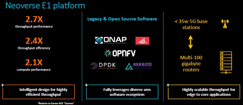
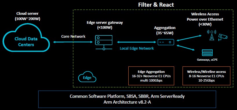
This SMT, as well as the mesh interconnect that Arm has created to glue cores together on a single die, will be big factors in boosting performance for edge devices like 25 watt to 35 watt processors in 5G base stations, other kinds of coprocessors and accelerators that sit in the datacenter, such as SmartNICs, and data transport devices like core routers with multiple 100 Gb/sec ports coming off their compute.
These are all part of the target market for the Helios E1 processor, according to Mohamed Awad, vice president of marketing for the infrastructure line of business at Arm, who talked about the potential uses cases at the recent Arm Tech Day in Austin.
“The E1 will support bot legacy and open source software, so it can quickly slide in and do OPNFV and ONAP and support DPDK,” explained Awad, using the alphabet soup for Open Platform for Network Function Virtualization, a reference platform created by and used by telcos and service providers, and for Open Network Automation Platform, which as the name suggests is an orchestration and automation framework in which to run network functions that used to be hardened into very expensive appliances from myriad vendors. DPDK is short for the Data Plane Development Kit, a packet processing engine created by Intel that has been open sourced and handed over to the Linux Foundation to manage and that now supports X86, Power, and Arm architectures. “If you think about the infrastructure from edge to core, there are a lot of appliances with software associated with them, and the Neoverse E1 platform that we are launching can support that legacy software but transition to this open source software.”
The scalability of the Helios chip will depend on how many E1 cores are meshed up and the inherent performance of the Helios core versus the “Cosmos” family predecessor, the Cortex-A53 that was popularly used in various network, security, and storage adapters and appliances. According to Awad, if you add up all of the processors used in the edge and in the datacenter, including 4G base stations all the way back to servers, storage, and networks in the datacenter plus all of those security and network appliances scattered around the datacenter and the edge, then Arm had about a 5 percent share of that aggregate computing back in 2011. And in 2018, when 300 million chips were shipped into this part of the IT sector, Arm had a 27 percent share and that share is still growing. (We presume these are revenue share numbers, therefore, but it would be interesting to see revenue share , given that there are many difference classes of machines. In the end, it is money that matters.) This chippery does not include WiFi routers or any gear that is in the last mile to homes or offices – it is the computational and storage edge. And, perhaps most significantly, that gives the Arm architecture the pole position among all chip makers – bigger than Intel, but we don’t know by how much because Arm did not share that data.
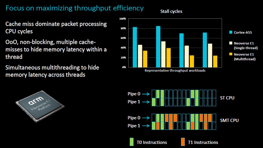
You may be wondering why Arm cannot just have a geared down N1 chip do all of these edge workloads. In a sense it has, but it takes more architectural tweaks than just cutting back the cores and caches and therefore the slots and watts. The compute to handle data transport workloads need to be able to handle a 10X growth factor over the next decade, according to Rob Dimond, system architect and distinguished engineer for the Architecture and Technology Group at Arm. If you do the math on that, this is about a 60 percent growth per year in throughput style processors – meaning ones geared towards heavily threaded software and relatively low power draw and not toward big fat cores with faster clocks and lots of cache, both of which generate a lot of heat.
The promise for the Neoverse N1 line, as we explained last fall, is 30 percent performance improvement per year at the socket level. Yes, Arm is demonstrating that it can do somewhere between 1.7X and 2.5X on various workloads running on the 64-core Ares chip compared to the earlier Cosmos Cortex-A73 processors, so it is a lot more than 60 percent growth out of the chute. And similarly, the Helios chips are delivering cores that run 2.1X faster and throughout that is 2.7X higher than the Cortex-A53 reference architectures, but that initial bump is probably not sustainable with each generation. And particularly if Arm tries to stick with an annual upgrade cadence for the E1 designs as it has promised for the N1 designs.
Drilling Down Into The Helios E1
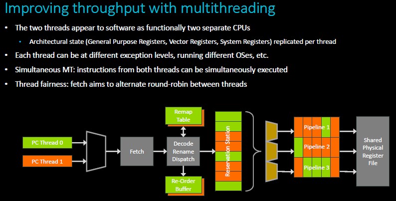
While the Ares N1 processor will support both 32-bit Armv7 and 64-bit Armv8 instructions, the 32-bit processing and memory addressing capability was jettisoned from the chip to save power and chip area in the Helios E1 processor and to make room for SMT, presumably. Here are the details on the SMT model that Arm has cooked up for the E1:
Over time, it would not be unreasonable for Arm to keep doubling up the SMT to four and then eight threads to try to meet that 60 percent performance improvement per socket goal. SMT8 really did work for the T series of chips from Sun Microsystems, when it was selling them, and it is still a very useful thing for IBM’s Power8, Power9, and presumably Power10 processors to boost throughput for workloads that like threads. Also, it would not be surprising to eventually see SMT appear in the Neoverse N2 or N3 or N4 processors in years hence.
By the way, the SMT on the E1 chip can be turned on and off with a software toggle, so for those workloads that would do better with a single thread per core running at a jacked up clock speed, it is possible to switch modes.
The whole E1 design is focused on balancing throughput in the socket against raw compute in the core, and to maximize the throughput per watt for those thready workloads that are expected out on the edge, in the datacenter data plane and control plane, and in server accelerators that have network, storage, and security functions offloaded to them.
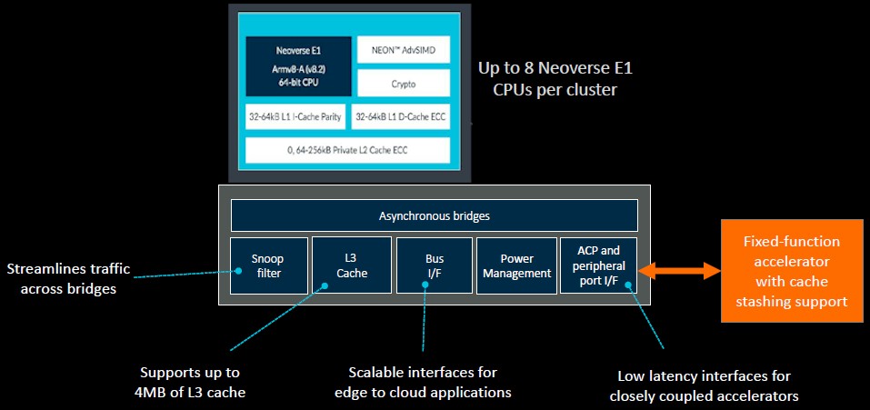
The E1 core has either 32 KB or 64 KB of L1 cache with parity checking and 32 KB to 64 KB of L1 data cache that has ECC scrubbing on it. Each core can also have from 64 KB to 256 KB of L2 cache front-ending the L1 caches, also with ECC scrubbing on it. The cores can have cryptographic engines and NEON AdvSIMD floating point units dropped in beside them as well, like this:
The E1 clusters can have up to eight cores on them with the Helios generation, and the circuits that wrap around the cores have asynchronous bridges that link out to up to 4 MB of L3 cache, various bus interfaces for peripherals, including those for fixed function accelerators as outlined above. You can have multiple clusters on an E1 chip, cookie cutting them onto a mesh interconnect. Presumably, customers could grab the cores and make a mesh interconnect between the E1 cores, as is done in the N1 designs, without clustering them, or break the clusters up into chiplets and use CCIX ports to link the chiplets together, as will also be done with the N1 chips. (We will have to see how Arm’s partners make use of all of these goodies.)
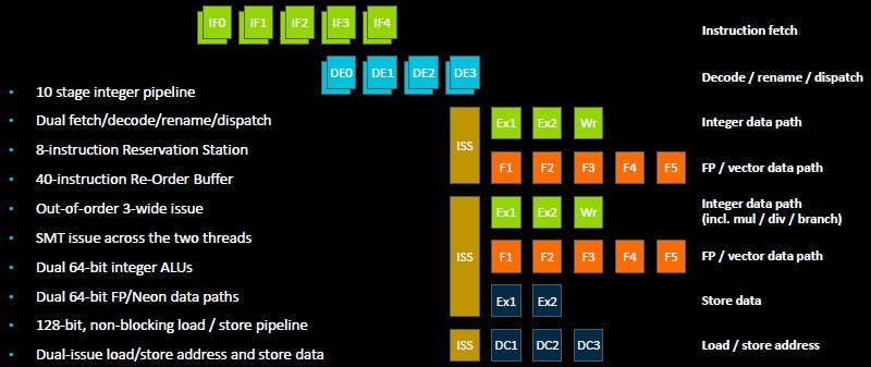
If you want to get into the core pipeline and compare and contrast it with that of the Ares N1 chip in the Neoverse line, here’s the block diagram for that:
There are a lot of differences between the N1 and the E1, and the big one in that there is a fixed 10-stage integer pipeline rather than the variable “accordion” pipeline that can scale from 11 stages back to 9 stages with the N1 chip. You can see the three wide pipeline and the two SMT streams that implement two 64-bit integer units with the pair of matching 64-bit floating point units.
The pair of floating point units are half as fat on the E1 as on the pair on the N1. That skinnier E1 math unit presumably will still be useful for mixed precision math relating to machine learning inference, given that everyone is expecting a lot of inference at the edge. The floating point units can together do eight FP16 operations per cycle, or four FP32 operations per cycle, or sixteen INT8 format “dot product” instructions per cycle. (That last bit is where the inference will most likely come into play.) If you look at the raw integer performance of the Helios E1 chip, it is 1.4X times that of the Cortex-A53 with threading turned off and 1.8X with the SMT2 turned on. With floating point, the performance boost is 2X between the Cortex-A53 and 2.4X with SMT2 activated.
When all is said and done, a reference core comes in at .46 mm2 in die size, and at 2.5 GHz implemented in the 7 nanometer process from Taiwan Semiconductor Manufacturing Corp, it burns 183 milliwatts. The reference design chip that Arm has put together for licensees to play with has a pair of eight-core clusters on it, linked by the CMN-600 mesh interconnect and two DDR4 memory controllers hanging off that mesh. The cores have a power budget of under 4 watts, and the whole system-on-chip burns less than 15 watts, has a SPECint_rate2006 of 153, and can push data at 25 Gb/sec, which is what a hyperscale datacenter server port does these days. In a small 5G cell base station deployment, one E1 cluster would be used for the control plane, the other for the data plane, and radios and security circuits would be added to the mix. This reference E1 platform running OpenSSL and DPDK on Linux in that small 5G cell base station would have 2.7X the performance of a similar platform based on the Cortex-A53 chip, and 2.4X better performance per watt.
Those are some pretty good compares, but the real test is how they stack up to real chips, especially the embedded ones that Intel and AMD are bringing to market to tackle the same edge workloads. We have not seen such comparative benchmarks as yet.
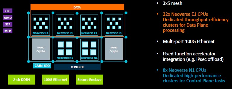
Here is another example of how packet processing on a software-defined network appliance might look with a mix of E1 and N1 processors implemented on a 3×5 mesh to create a high throughput data plane running on the E1s with the beefy control plane running on the N1s, and thus be able to do packet processing at 100 Gb/sec line speed:
We can imagine all kinds of uses and all manner of configurations that the E1 and N1 chips might be put to use in. The question now, as always with the Arm collective, is this: What partners of Arm are going to do what to actually get chips based on this innovative technology to market? Moreover, how much will they be tempted to fuss with it? Hopefully there will be many partners, and less fussing. Time is of the essence.




It’s very wrong to compare the E1 to A53. In it’s base E1 is A55 with basic OoO scheduling and SMT. The cluster & topology is also already seen DynamIQ one with no changes, the N1 return to micro cluster per two core’s is much more advanced regarding power consumption control but we still need to actually see how much did ARM menaged to fix performance regression caused by shared cache lv especially for FP SIMD instructions in such implementation. With enabled SMT it matches the performance of A72, A73 so it should really be compared with A73 as a newer & more efficient of those two. The real question is how much smaller is E1 footprint on silicon & how much more power efficient is it compared to the A73. Judging by ARM data not much & only in ideal SMT conditions. I think ARM missed the target with E1, it could turn the things around with adding scalable vector extension & optimising the cache for 512 bit SIMD. I am also curious about the implemented SMT implementation, the MIPS showed VSMT implementation that was very efficient (small and easy to implement) with similar performance benefits. At the end you win some & lose some, back to drawing bord.
Five years of Xeon volume data for estimating traditional segment displacement potential in units, and data for into future revenue calculation are here:
https://seekingalpha.com/instablog/5030701-mike-bruzzone/5272437-xeon-channel-inventory-management-data
Mike Bruzzone, Camp Marketing
Several corrections:
-Modern Atom is out-of-order, and has been for many years (since Silvermont came out in 2013.)
-Modern Atom, in server configs, does not have SMT; only the Xeon Phi “Knights Landing” chips do. Mainline Atom abandoned SMT when they went to OoOE.
-Out-of-order debuted originally on the Pentium Pro, not on RISC chips. Metaflow announced but did not release OoO SPARC cores prior to the PPro.
-“Cosmos” doesn’t refer to A73, as A73 never seems to have been used in the infrastructure market, and the performance comparisons were definitely against the A72 – not the A73. https://images.anandtech.com/doci/13959/04_Infra%20Tech%20Day%202019_Pellegrini%20Workloads_FINAL%20WM6.jpg
-“Other vendors can do four-way or even eight-way SMT, but Intel has always opted for two-way SMT.” This is especially weird to say in the context of Atom, since the only modern Atom cores with SMT – Knights Landing – have 4-way SMT.