
It is no secret that Intel has been working to get its “Cascade Lake” processors, the second generation of its Xeon SP family to market as early as possible this year and to ramp sales at the same time that X86 server rival AMD is expected to get its second generation “Rome” Epyc processors in the field. It looks like this Cascade Lake launch will be happening sooner rather than later.
For one thing, the invitations have gone out for Intel’s Data-Centric Innovation Day on April 2 in San Francisco, which will be hosted by Navin Shenoy, general manager Intel’s Data Center Group, and Lisa Spelman, general manager of Xeon processors and datacenter marketing. This strongly suggests that there is a looming Xeon announcement, and the name of the event suggests, as did last year’s Data Center Day event, that Intel will be making a broad set of announcements for all kinds of things, including various kinds of compute, storage, and interconnect. This is just how the chip maker rolls in the years since Intel Developer Forum was mothballed.
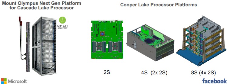
Moreover, at the Open Compute Project’s Global Summit in San Jose a little more than a week ago, Jason Waxman, who sits on the OCP board and who is data centric chief strategy officer and general manager at the Datacenter Solutions Group at Intel, was showing off a super-dense quad-socket machine based on Cascade Lake as well as future machines with two, four, and eight sockets based on the follow-on “Cooper Lake” processors expected later this year.
The Cascade Lake chips are a tweak to the current “Skylake” Xeon SP processors, and they are socket compatible with Skylakes as will be the future “Cooper Lake” Xeon SPs that will follow relatively fast on the heels of the Cascade Lake processors later this year. Both Cascade Lake and Cooper Lake are being etched with a refined 14 nanometer process that allows Intel to squeeze out more performance and more thermal efficiency out of the Xeon SP family. The main difference in the architecture coming with Cascade Lake, aside from hardware-based mitigations to block the Spectre/Meltdown side channel speculative execution vulnerabilities that hit the CPU industry in January 2018 and support for Optane 3D XPoint persistent memory in DIMM form factors sitting beside normal DDR4 DRAM, is a new set of instructions called various Deep Learning Boost (DLBoost) or Vector Neural Network Instructions (VNNI), which were originally slated for the Skylake Xeon SPs but didn’t make the cut. As we explained last summer, VNNI allows 8-bit integer data formats and instructions to be pushed through the AVX-512 vector units in the processors, allowing them to crank through four times as much data as was possible with 32-bit single precision floating point. This has radically sped up machine learning inference workloads.
With the Cooper Lake chips coming later this year, which can also plug into the Socket R sockets used by the Skylakes, the big change will be the addition of support for the bfloat16 format that Google created for the third generation of its Tensor Processing Units (TPUs) and that is also used in the Nervana neural network processors from Intel. Bfloat16 is interesting in that this format can express the same range of numbers as an FP32 number using a slightly tweaked exponent and mantissa but it only uses 16 bits like half-precision FP16 floating point. (We explained bfloat16 back in December when Intel rolled out some more pages in its Xeon roadmap and talked about its future Xe discrete GPUs.)
That sets the stage for what Waxman talked about at OCP Global Summit, and one of the key things that the OCP community wants is integrated solutions, which is just a way of saying consistent and standardized assemblies of components that can be replicated by many vendors without what Facebook has called “gratuitous differentiation” that is more about helping the vendors than helping the customers. The community is also calling for systems that are optimized specifically for workloads, and that means adding a diverse set of systems to the datacenter rather than just a few SKUs that frankly do not run all software equally well. The days of a single compute substrate are fading pretty fast in the face of a slowing Moore’s Law pace in the density and cost reduction of chip manufacturing. (The fabs go up in price proportionately as the transistors go down in price, and both are getting more costly at an increasing rate as we hit the limitations of atomic physics.)
Waxman threw Microsoft Azure’s Project Olympus systems a bone in the presentation, saying that they would be tweaked to support the Cascade Lake processors and the “Apache Pass” Optane 3D XPoint persistent memory that is being added to the “Purley” platform. And again, Optane PMMs (short for persistent memory modules) were supposed to be added during the Skylake generation, but 3D XPoint did not have the yields or speed that servers demanded when the Skylake Xeon SPs were launched in July 2017. Once the Optane 3D XPoint missed the Skylake boat, it was a good idea to use it as a means to boost sales of Cascade Lake and follow-on processors. It’s not like anyone else is putting persistent memory in DIMM form factors out; Micron Technology will probably do it eventually, and other makers of PCM memory could as well. But for now, Intel will have the market all to itself.
As for the Cascade Lake processor that Microsoft is adding to its Olympus machines, all that Waxman said was that Intel would be “launching this relatively soon.”
“We are also seeing a need for more scalable platforms, and this is relatively new for the OCP community,” explained Waxman. “We know that one-socket and two-socket platforms have been the bread and butter, mainstay of the community, but we see workloads that require bigger scale. So with the Cooper Lake platform, we want to be able to deploy reference designs that are scalable. They can have two sockets, or four sockets, or eight sockets, depending on the configuration. And the goal is to be able to have a large memory footprint and a lot of compute as a result.
Not for nothing, but this is how IBM has been building Power-based NUMA machines since the Power5 systems back in 2005. . . .
Intel is collaborating with Facebook on creating a line of servers that have two, four, and eight sockets and that are specifically designed to use the future Cooper Lake Xeon SP processors. It is not clear if this is the same architecture as the CPU portion of the “Zion” hybrid CPU-GPU machine that Facebook unveiled at OCP and which we discussed last week. It looks like a denser derivative, based on the mechanicals shown above, but that could just be distortion of the images.
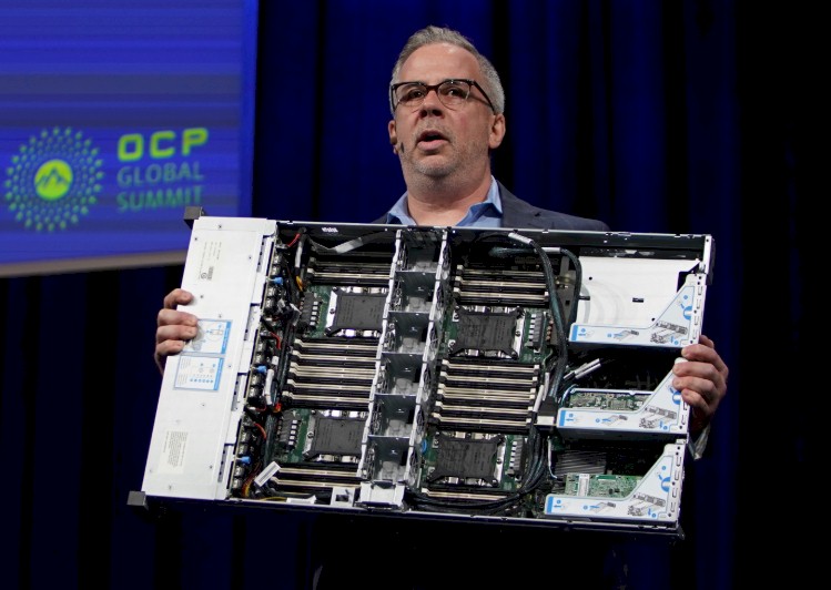
The more immediate machine that Waxman revealed during show and tell at OCP was a super dense system optimized four processor sockets, which he said was new in the OCP industry and “game changing.” Not for nothing, but Intel and its partners have been shipping the Xeon E5-4600 family of processors for superdense four-socket machines since the “Sandy Bridge” E5-4600 v1 processors debuted in May 2012, two months after the Sandy Bridge E5-2600 v1 processors for two socket machines came out. The Chinese hyperscalers caught four-socket fever way back in the wake of the Sandy Bridge launch, in fact, and often half populated their machines with the idea that they could add memory and CPUs later and double their compute rather than throwing out the iron.
In any event, this four-socket machine is about providing more virtual machine density, according to Waxman, and by that he doesn’t necessarily mean more VMs per system but also VMs that are themselves more dense, possibly eating the whole machine to run an instance of SAP HANA, for example. Here is Waxman hefting this four-socket Cascade Lake reference beast, which was contributed to OCP by Intel and Inspur:
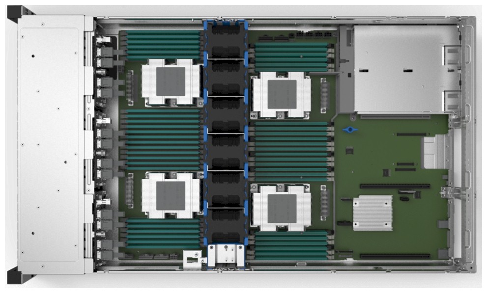
And here is a top down clearer picture of this four-socket system:
The machine will be available in the second half of 2019, and in addition to Inspur, other server makers, including Dell, Hewlett Packard Enterprise, Hyve Solutions, Lenovo, Quanta, Supermicro, and Wiwynn are planning to make machines based on this reference design.
This four-socket beast will able to support up to 12 TB of Optane PMMs across its 48 DIMM slots (twelve per socket). You have to have some DDR4 memory in a system to boot, so such a machine cannot be using 256 GB Optane PMMs (256 GB times 48 slots is precisely 12 TB). Therefore, this system must be using 512 GB Optane PMMs, and that means it has 24 slots allocated for DDR4, which can be anywhere from 32 GB to 256 GB in capacity, but in the real world hyperscalers will go for the sweet spot in the market and use 128 GB DDR4 sticks. So that is 3 TB of main memory and 12 TB of Optane PMM memory for an effective memory capacity of 15 TB. We are dying to know how this system would perform compared to an all-DDR4 machine and what the price difference and price/performance difference will be with an all-DDR4 setup.
There seems to be some confusion about whether or not this system supports the two-chip Cascade Lake-AP processor, which will put two Cascade Lake chips into a single socket to jack up the core counts and the overall throughput. Intel divulged the doubled-up Cascade Lake-AP chip last fall ahead of the SC18 supercomputing conference, and at the time would be putting two 24-core Cascade Lake chips into a single socket, thus allowing for up to 12 memory channels to be hung off each socket in the system. In theory, as we pointed out at the time, Intel could match the eight DDR4 channels per socket that IBM Power9, AMD Epyc 7000, and Marvell ThunderX2, and Ampere eMAG 1 processors and still have four left over either for more memory or for the attachment of Optane PMMs. Depending on the clock speed, this Cascade Lake-AP chip could burn anywhere from 275 watts to 350 watts, and the consensus on the street for months has been that it will be at the upper end of that range because Intel is pushing up the clock speeds more than it might otherwise because of the competitive threat with AMD’s Rome Epycs.
Here is our point. Waxman said that this four-socket Cascade Lake reference machine would have 112 cores, and that means 28 cores per socket and that means it is using a plain vanilla Cascade Lake chip, not the Cascade Lake-AP, which would cram 192 cores (48 times four) into that 2U form factor. We are not saying that Intel could not work with the hyperscalers to create a version of this system that did use the Cascade Lake-AP processor, but it would probably not be air cooled and would need heat plates at the very least and possibly full-on liquid cooling in that 2U form factor. If you put such a Cascade Lake-AP it in a 4U form factor, you might as well just use a regular four-socket box and not bother with all of the engineering. It comes to the same density, and the only benefit is cutting down on power cables and power supplies.




Gold 6248, a 20C, is the first to hit the channel last week, primary beta validation grade at 20C(?). Ask $2299 used to $2700 new. 20C Skylake cost Intel $215.63 each on average. Means these are monopoly price premium parts at $1K.
Mike Bruzzone, Camp Marketing