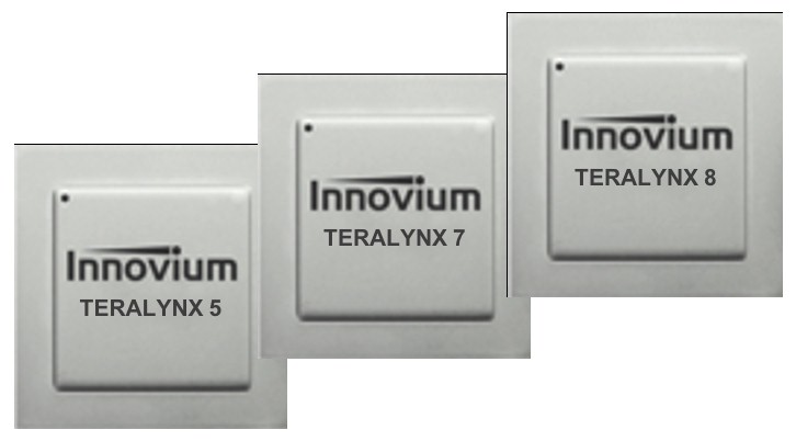
There is a relentless hunger for bandwidth in the largest datacenters of the world as well as a desire to flatten networks and thereby reduce latencies and the cost of the networks that interconnect servers and storage to provide modern applications. In the past decade, competition has been good in terms of picking up the pace for Ethernet bandwidth increases and using Moore’s Law and clever designs to drive up the switching density of devices.
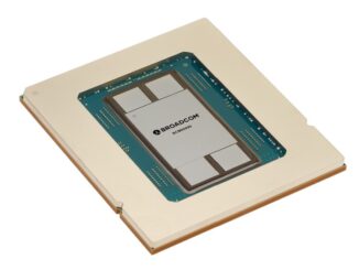
Here in 2020, at the beginning of a new decade, there is no sign that this pace is abating, with Innovium launching its Teralynx 8 chips hot on the heels of merchant switch ASIC industry leader Broadcom, which rolled out its “Tomahawk 4” StrataXGS family of chips back in December 2019. The Tomahawk 4 chip has 512 SerDes running at 25 GHz with PAM-4 encoding delivering four signals per lane and two bits per signal for an aggregate of 50 Gb/sec per lane, which is an aggregate of 25.6 Tb/sec across the Tomahawk 4 chip, which is a monolithic die and just about busting out of the reticle limits for the 7 nanometer processes at Taiwan Semiconductor Manufacturing Corp. Innovium is driving its switch ASIC designs a bit differently, moving to SerDes that have a native speed of 50 GHz (after encoding and error correction overhead is taken off) and then adds on PAM-4 data encoding to double up the effective data rate of the lanes and then only needs 256 SerDes to achieve the same aggregate 25.6 Tb/sec switching bandwidth across the Teralynx 8 chip that is being unveiled today.
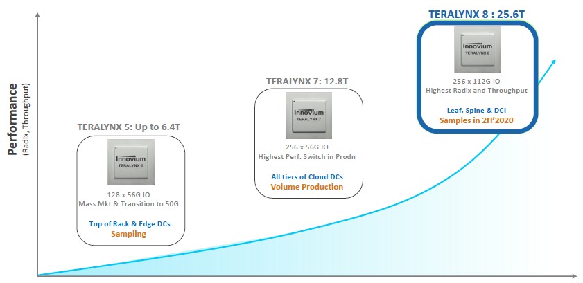
The Teralynx 8, like the Teralynx 7 launched in April 2018 and the Teralynx 5 launched in September 2019 at our The Next I/O Platform event in San Jose, are both monolithic designs, and like Broadcom, Innovium is putting off moving to a chiplet architecture, gluing together multiple chips to create its switch ASIC, until the last possible moment. The Teralynx 7 chip, which was the former flagship datacenter product from Innovium, is ramping nicely, Rajiv Khemani, co-founder and chief executive officer at Innovium, tells The Next Platform and the Teralynx 5 is sampling now (with the A0 stepping no less) and getting ready for its own ramp as an ASIC for top of rack switches and edge datacenters. Being cryptic and not wanting to give out port or switch ASIC numbers, Khemani says cryptically that over 2 million PAM4 SerDes lanes per quarter are shipping from Innovium and that number is on the rise.
The Teralynx 7 chip is being resold by a number of OEMs and ODMs, including Cisco Systems, which has it inside of its Nexus 3400-S switch. Khemani says that “more than ten of the top fifty” hyperscalers, cloud builders, and service providers in the world are using Teralynx 7 ASICs in their switches, and furthermore two of the top five hyperscalers and cloud builders are using Teralynx 7 ASICs. Cisco’s NX-OS runs on the chip, and so does Microsoft’s SONiC switch operating system and so do a number of homegrown network operating systems from the hyperscalers. That is not bad market penetration for an upstart that just uncloaked two years ago.
Innovium has raised $250 million in five rounds of funding so far, including money from Walden Riverwood, Greylock Partners, Qualcomm Ventures. Redline Capital, Capricorn Investment Group, Paxion Capital, and DFJ Growth. About $100 million of that is left, and $50 million to develop each of three chips is a pretty low cost in the scheme of semiconductor things. The company has opened a research and development lab in Portland, Oregon recently, adding to the facilities it already has in Bengaluru, India and San Jose, California; it also has sales and support teams in China and Taiwan and now has more than 180 employees.
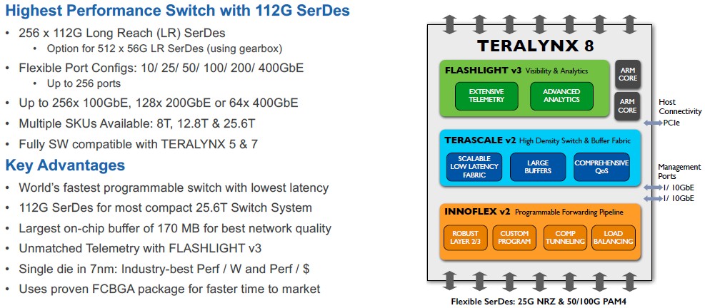
The Teralynx 8 chip has 112 Gb/sec native, 100 Gb/sec actual SerDes operation, and at 450 watts, this is a very hot chip that is going to deliver a lot of port density and radix or raw bandwidth, depending on how this bandwidth is sliced and dices by switch makers.
“We are finally getting to the point where the SerDes is catching up to the optics,” explains Khemani. “As you, in the last year, optics has moved to 100 Gb/sec lambdas and it has taken a few years, but the Serdes are catching up to the optics. And that is obviously good from an overall systems and deployment standpoint.”
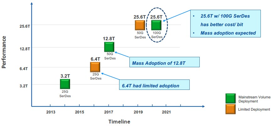
Khemani says that the 3.2 Tb/sec ASICs from Broadcom, Innovium, Mellanox, and others, which hit the market around 2014 or so, covered the sweet spot in the market in terms of performance, price/performance, and port density for the time. But doubling up the Serdes count and keeping the 25 Gb/sec SerDes the same was not widely adopted and that when the industry moved up to 50 Gb/sec SerDes and delivered 12.8 Tb/sec ASICs, these were more widely adopted. Innovium is hoping that this pattern repeats itself, especially since Broadcom’s Tomahawk 4 stuck with 50 Gb/sec SerDes and doubled them up to get to 25.6 Tb/sec and Innovium has move dup to 100 Gb/sec SerDes to do 25.6 Tb/sec switch ASICs. It really comes down to the cot per bit getting low enough at the same time the market is ready to move to a faster switch.
“If you are building a next generation datacenter, you have a choice,” he says. “Do you stick with the 50 Gb/sec SerDes or do you go with 100 Gb/sec SerDes? If you are making a new design and making a new infrastructure decision right now, you ought to bet on and pair with 100 Gb/sec optics. That we believe is going to be a mainstream deployment as we go forward.”
The Feeds And Speeds
It has been a long time since we have seen a chip shot of a switch ASIC, and Innovium didn’t share one for the Teralynx 8, either. What we can tell you is that Teralynx 8 is aimed at leaf, spine, and datacenter interconnect (DCI) switches and that it will be sampling in the second half of this year. Here are the basic feeds and speeds of the device:
The Teralynx 8 is fully software compatible with the prior Teralynx 5 and Teralynx 7 chips, but it is not pin compatible with either chip. It has an FCBGA package, not the kind of LGA sockets that CPUs and GPUs sometimes use and that are being adopted by other switch chip makers. The three different SKUs of the Teralynx 8 offer 8 Tb/sec, 12.8 Tb/sec, and 25.6 Tb/sec of aggregate bandwidth and they are pin compatible with each other. The two faster chips have 170 MB of on-chip buffer capacity while the slowest variant has only 114 MB. Either way, that is a pretty big gob of cache, and it is especially needed on hyperscaler and cloud builder networks that have a certain amount of congestion and still they don’t want to drop packets – at least not all the time.
“The size of the buffer matters a lot,” says Khemani. “It reduces packet drops and it allows you to handle many simultaneous flows and essentially deliver a better quality network. The deep buffers are typically used when the switches are facing the WAN, and often for datacenter interconnects and they prefer to use the same chip for all of these roles – especially when they have such large buffers.”
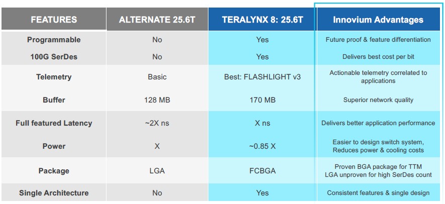
Here is how Innovium stacks itself up against the Broadcom Tomahawk 4, although it doesn’t mention its rival chip by name:
The big bad Teralynx 8 weighs in at less than 500 watts, based on pre-silicon estimates, which is around half again as hot as the 300 watts of the Teralynx 7 but apparently around 15 percent less hot than the wattages that Innovium reckons the alternatives will come out at. As for latency, Khemani says the typical port to port hop is on the order of 500 nanoseconds, but for typical alternatives it is more like 1 microsecond; the important thing is that this number is much lower than what Tomahawk 4 will deliver. The on-chip buffers are 33 percent larger than the 128 MB in the Tomahawk 4 as well, which as we noted, is key for hyperscalers and cloud builders who are obsessed with quality of service.
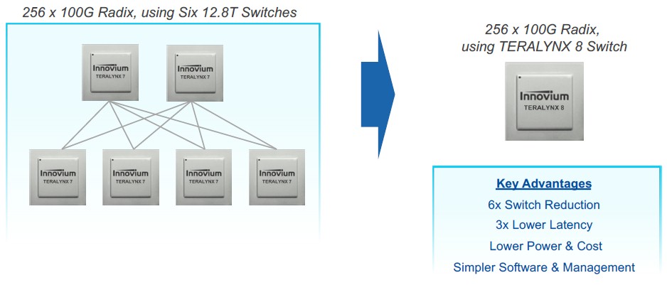
While bandwidth is great, flattening the network is sometimes more important, and the same ratio of network collapse holds for Innovium’s Teralynx 8 compared to its Teralynx predecessor as for Broadcom’s Tomahawk 4 compared to its Tomahawk 3 predecessor:
If you want 256 ports of non-blocking connectivity using the prior generations of 12.8 Tb/sec devices, you need six chips to do the job. The new 25.6 Tb/sec ports can do that with a single chip. And even if that chip costs 2.5X to 3X as much, there is a huge savings in switch installations and a big reduction in latency because it takes fewer hops to do the connections. Or, companies can make their networks larger, of course, although no one seems to want to do a datacenter that has more than 100,000 servers and storage servers, and the largest actual clusters doing real work as a single entity tend to be on the order of 50,000 machines. There seems to be more appetite for using the bandwidth to boost the radix of the switch and flatten the network, and 100 Gb/sec split down to either 50 Gb/sec or 25 Gb/sec ports down to the servers and 100 Gb/sec ports across the leaf and spines higher up in the network seems to be the design of choice.
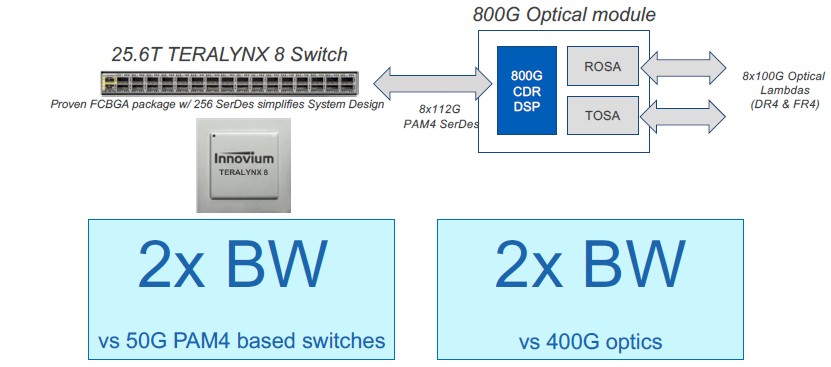
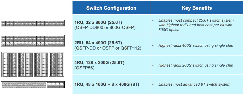
There are some implementations that will roll out 200 Gb/sec, 400 Gb/sec, or even 800 Gb/sec ports, of course. And Innovium can support these with Teralynx 8:
The interesting thing to consider how fast a 1U switch with 32 ports can go over time in a relatively affordable package. Back in 2012, that was a 40 Gb/sec speed, and by 2015 that jumped to 100 Gb/sec. When Innovium jumped into the market in 2018, then its switch partners could do 400 Gb/sec on those 32 ports crammed into a 1U form factor. And by the time the Teralynx 8 is shipping in products early next year or so, it will be 800 Gb/sec ports. The Teralynx architecture as implemented can double up again to 51.2 Tb/sec (our guess is by doubling up the SerDes count using a 5 nanometer process) and push that up to 1.6 Tb/sec per port.
We live in the future.
Innovium is taking orders for Teralynx 8 evaluation systems and chip samples now, and expects to ship the samples in the second half of 2020. The hardware design collateral and software design kit for Teralynx 8 will be available soon.



Be the first to comment