
Let’s leave aside all the questions about the long-term viability of AI ASICs and appliances and focus instead on the beauty of a good architecture. Because ultimately, that’s what some of you are here for, right?
Just because something might not stand the test of time, especially against fierce general purpose accelerator competition (and a hyperscale market that will just build it themselves) doesn’t mean it’s not a credible rival for at least some slice of the pie. And when it comes to AI training at scale, Nvidia has some mindshare competition for those willing to go a different direction—and Graphcore appears to have a well-lined path for the brave and time-endowed to follow.
Back in the good old days, before the truly unique architectures for training/inference were snatched up and shortly after the world figured out these were just a bunch of a matrix math engines with barely cooked software stacks to support them for real work, AI chip startups had a good run. We profiled Graphcore early and continued watching as they snagged a few customers and more important, racked up what seemed like endless venture capital, still seems like it, actually. If the costs of bringing a chip to market are anywhere between $50-$100 million, Graphcore should be bringing something remarkable to the table—many times over, in fact given their cumulative $460 million in funding over 5 rounds to date.
And lo, their second generation architecture, the one they meant to build all along, as CEO and co-founder Nigel Toon tells us, has arrived. One of the surprises here, which felt like a treat after years in the price-less desert of such silicon upstarts, is that they released system cost—enough to do some price/performance analysis and pull apart some reasonable compares. That alone is guaranteed to get them some traction with the new wares out of the gate.
(Challenge question on above pricing: if you separate out, even with rough mental math, all of the components, especially on the networking side, what is your best guess for the cost of just the compute and how does that compare to the cost of an Nvidia A100 GPU?)
Now, back to the part above about the architecture being what you’re here for (the part that’s hard to get to in any AI chip startup story because the difficult business case problems are so profoundly distracting and even further complicated when a company raises so much money for a customer base that even at best will dwarf what the general purpose accelerator market will claim since the only users with enough volume to make it all work build their own stuff).
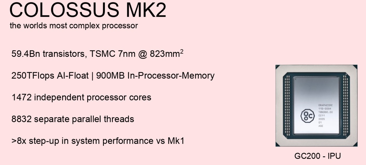 The 7nm device is dense with 59.4 billion transistors inside each of the new Mk2 IPUs and just under 1500 separate processors inside each chip. Graphcore has also made the expected leap with the new process to more memory—3X more, for a total of 900 MB inside each, enough to hold large models inside the processor, a big advantage, especially for the NLP (and similar) models Graphcore wants to snag from Nvidia. Toon says the new device is an 8X-9X (depending) leap over the previous generation (PCIe card) but as in deep learning overall, compute is just one part of the requirement, and a relatively easy one at that.
It’s the data fabric they’ve been developing that’s worth mentioning in more detail. Toon says the Oslo-based team that developed it is comprised of ex-Sun folks who went on to build large scale-out machines at Oracle. More specifically, the interesting part is the interplay between the memory, the software stack/compiler, and the fabric. With Mk2 Graphcore introduces IPU Exchange Memory, the IPU fabric, and features baked into their Popular stack to elegantly support sparsity, especially in the large-model and dynamic spaces.
Graphcore has built an IPU gateway it says can support many thousands (up to 64,000) IPUs working together and can connect IPU machines directly (box to box) and through switches for even larger machines. “Unlike normal Ethernet switching where everything connects to everything, that’s not required in AI so we built a ring system for communication and support collectives to reduce operations/communications required and power taken by the communications piece.”
The fabric itself is basically a standard 3D torus; one dimension is the IPU links between chips which were already there, another goes through the IPU gateway (the new chip they created to serve as the low-latency switch) for the second. And the third dimension is the IPU itself. “What you have is a 3D torus that’s moving data around, sharing weights across IPUs across the model if you’re training and has the collectives and all-reduce operations built into the fabric so that’s running in parallel with the compute on the IPUs.”
 The value of a 3D torus is hard to argue with, we’ve seen this before on old fashioned machines like the BlueGene Q, come to think of it. In the case of Graphcore’s machines, instead of connecting all to all through some kind of Clos switch networking structure with all of its power and switching layer demands, the torus runs across an array of IPUs that can break and rejoin those loops at any point, which allows for dividing the large rack system up into multiple domains of IPUs.
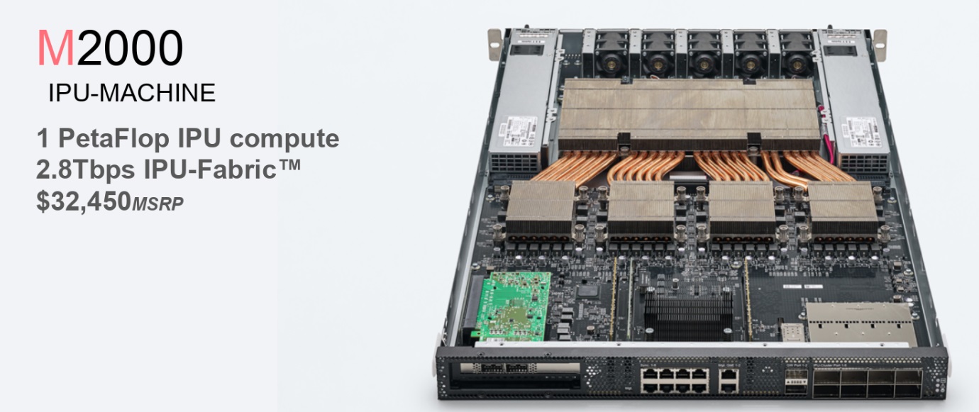
All of this; the IPU machine, the DRAM and IPU gateway, amount to one petaflop inside the 1U box with all the network inside. “All you need to do is connect with standard Ethernet (standard NIC card) or direct connect to a server or use a SmartNIC. “Because of disaggregation of the CPU you can change ratio of IPUs to CPUs depending on the application,” Toon adds. There is also a Virtual IPU layer that works with workload managers like Slurm or orchestration platforms like Kubernetes to allow reuse of IPU systems in different ways.
Each of the IPUs can address up to 450 GB (DDR4 DIMMs so there are options). The Poplar software stack takes the graph from TensorFlow or PyTorch and expands it into a full compute graph that exposes compute, data, and communications, so with those three streams it load balances the compute across the parallel compute threads and orchestrates the data so it’s in the right place at the right time and manages communications between those program threads (on single IPUs or across a training system).
The new IPU Exchange Memory feature uses Poplar in way similar to cache in theory (the data needed for compute is inside the processor) but in this case, whereas a cache is trying to decide what’s relevant in the future, Poplar program, data, communications, etc. are all compiled up front so the stack knows what data is required and when and can make sure the data is available inside the processor.
With 900 MB to work with there’s quite a bit more capability. “From that point of view it’s like having a perfect cache,” Toon says. “As far as processors are concerned, they always see data in the local SRAM next to the program thread, spread across the four IPUs inside the IPU machine; that’s 180 TB of bandwidth the program has available to it, then you get this incredible bandwidth but you also get access to all that data.”
“But”
The IPU and system are designed to tackle sparsity and have the memory profile needed for large model sizes and those with complex requirements. The price makes sense competitively. The topology is reasonable and elegant. The software stack seems well developed and with ease of use in mind. Scalability is impressive. Leadership and pedigree are sound. None of these are issues.
But here is the issue, the only one that matters.
This machine cannot do anything else.
It can excel at AI training, especially for important target areas in NLP, for instance, where models need ample memory tied to compute. It can also do inference, although what can’t, really?
The real barrier has nothing to do with this system or its elegant network and compiler or Graphcore at all.
It is a question of what room there is for even the best engineered AI specific system architectures to take on general purpose accelerators and if not those, then systems that can handle everything seamlessly, from HPC simulations to low-precision training or inference to transactional processing if it came down to it.
It’s been almost five years that we’ve watched the first AI ASICs spring forth and to date, none of them have really succeeded in capturing significant share. It was easy to say then that it was too early, then that most of the truly unique, inspired architectures had been acquired and subsequently squelched. But now, as the world decidedly is not the mood for anything that adds new potential complexity, even at slightly lower cost or slightly higher performance or efficiency, we can officially declare the AI chip startup party is over. Because now, as we see with Graphcore (and it’s unfortunate their news became the springboard for all of this) even an elegantly designed, well-considered architecture that is backed by many millions of dollars is going to have a tough uphill climb. In short, quality, creativity, and even a meaningful edge aren’t enough to make a dent. After all, this is still a volume market where the volume-makers will build their own well before they buy anyone else’s. Is it possible an Amazon might come along and give a Graphcore a go and chuck the many years of CUDA expertise it has cultivated internally? Sure. We hope so. Is it likely? You decide. And does one hyperscaler a business make? You decide.
2015 was a hopeful time for new purpose-built architectures and there was no more striking problem at the time than deep learning. 2017 was similar and there were all kinds of new architectures to explore, many of which on closer inspections were just very similar matrix math units with varying degrees of “magic compiler” backends that we still haven’t completely been able to see into. By mid-2019 the party was actually over for training and while inference is anyone’s game, the architectures are far less interesting (for big infrastructure folks) and the margins much (MUCH) lower. Where’s the fun in that when your company wants to pitch us on datacenter inference when it fact it was really designed for the only viable market—a digital camera or drone or some other nonsense.
And sadly, for those who dig the hardware, AI innovation will be in the frameworks and algorithms, that’s where the next wave of elegance will come from. That will play out on systems that can weave between doing a lot of things well instead of just one thing (training), which could very well change completely in the next couple of years.
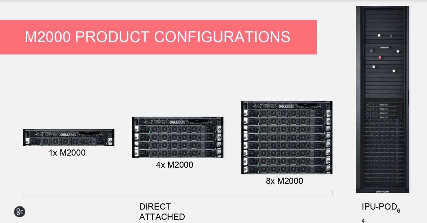
Let’s close with some possible configurations, shall we?

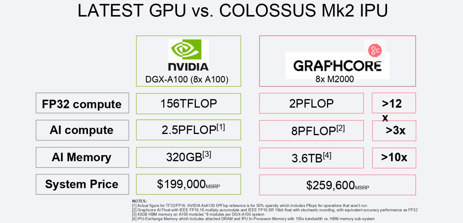


Scathing, but realistic. There are some other caveats I think are worth mentioning concerning their DGX-A100 comparisons.
Firstly, the DGX-A100 is a server. 8X M2000 needs to be attached to an existing server. You need at least one server for every 8 M2000s and the price they have listed is just for the M2000s. “Poplar will just see what’s connected.” I can’t imagine there isn’t tuning necessary, choosing what sort of server you need to not hold back your compute. It also needs to be integrated whereas that is done for the DGX-A100.
Secondly, the 3.6 TB of “AI memory” is mostly DDR4 memory, which they say streams. Does it stream fast enough to keep the 8 PFLOPS fed? Perhaps, but that is something that must be demonstrated.
Thirdly, the “AI Compute” uses TF32 for the A100 and 16 bit mac for the M2000. Graphcore claims the stochastic rounding they use provides training accuracy equivalent to FP32. Is that always the case? It must be demonstrated. But BFloat16 is also meant to provide training accuracy equivalent to FP32. I am sure porting one’s training code to FP16 on an M2000 demands a lot more code changes than changing from FP32 to BFloat16 with CUDA. NVIDIA’s A100 offers BFloat16 performance at twice that of TF32, so it seems to me the proper “AI compute” comparison should be 5 PFLOPS for the A100 to 8 PFLOPS for the 8x M2000, not 2.5 vs. 8 as in their chart. Who knows what real-world performance differences there are. I can certainly imagine, assuming their memory streaming works well, that the real world difference could be even more in favor of the 8x m2000s than the 2.5 vs. 8 in many contexts. But as far as the peak theoretical numbers they are comparing I think they chose the wrong one.
Thirdly, for the “FP32 Compute” they compare general purpose CUDA core compute to whatever FP32 compute the M2000 can provide. And what can it meaningfully provide anywhere close to the 2 PFLOPS throughput claimed on the chart other than FP32 matrix multiplications (is their caching system sufficient to stream 32-bit GEMM at that throughput?), perhaps even limited by support through Poplar to training FP32 AI models? That’s a silly comparison. Here, Graphcore seems to be trying to make a marketing bullet based solely around the fact that NVIDIA doesn’t provide any strictly FP32 Tensor Core support. But for anything the M2000s are going to be used for, the proper comparison would be to NVIDIA’s TF32 Tensor Core support, which would be 2.5 PFLOPS for the A100 versus 2 PFLOPS for the 8x M2000s. The fact that Graphcore even included FP32 support suggests they don’t think they can convince people that FP16.16 with stochastic rounding is all they need for AI training.
Well written Nicole and thanks for the comment Matt! Although I wouldn’t yet throw in the towel on the upstarts. AI training and Inference certainly demand a significant share of their capex wallets and while the Hyperscalers have the resources to develop their own, when the time is right, it would be a lot easier for them to pick up one of Graphcore, Cerebras or Sambanova when the timing and valuation are right. And valuation is an entirely separate world – we are in funny-money times, so who knows.
The basic problems with a general purpose accelerator are several-fold:
1. Efficiency is directly impacted by generality – you can’t create a super-efficient computational engine if you also want to make it full general. A purpose-build video codec or AI engine will always be better than a more general-purpose FPGA, CPU, or GPU implementation of the same.
2. Programmability is directly impacted by how much hardware is dedicated to supporting common programming models. General purpose CPUs are tremendously programmable, but this is because they devote literally 95% of their non-SRAM silicon to hardware that makes sequential programs go as fast as possible. The downside of this approach is that the above-mentioned 95% of the silicon is not actually exposed to the programmer nor usable to actually compute anything of value. FPGA’s have the potential for much higher performance, but because they devote very little hardware specifically to supporting arbitrary programming models, and all the hardware is available to apply to compute actual results. However, due to their architecture, they are tremendously difficult to program and end up requiring close coupling with a CPU to offload the tasks that are painful to implement in the FPGA fabric.
3. Volume is critical to being able to take advantage of the most advanced fabrication processes. Highly tailored compute engines by definition cannot take advantage of as much volume. And in the end, if you end up implementing a highly specialized accelerator in 28nm and compare it to a more general purpose solution in 5nm, the more general solution is going to have better performance and have the volume. The hope was that AI training would suck up so many compute cycles that it would generate huge volume requirements, but so far, this hasn’t really translated to the startup silicon world. Betting on Nvidia is just much more palatable for most orgs which have the money to spend on hardware.
If there were a new architecture with the nearly the same programmability as a CPU but with fine-grained parallelism and fully-programmer-exposed hardware of an FPGA, it might have a chance to succeed, because it would be substantially more efficient than a CPU, much easier to program than an FPGA and would be able to address a much bigger market to allow bigger volumes.
The M2000 specification is some kind of misleading: it is said the Exchange Memory is 450GB in capacity and 180TB/s Bandwidth. but it seems the 180TB/s is referring to the on-chip SRAM bandwidth (47.5TB/s per IPU and 47.5TB/s x 4 = 190TB/s) and the capacity is referring to external /Host DRAM via PCIe Gen4 X16 that is max 64GB/s theorically. So the 450GB and 180TB/s are not referring to the same physical thing. Am I right? Don’t like this kind of marketing misleading information on the product specification.
Yeah, their marketing is a bit misleading. Anything over 500GB/sec off chip requires HBM memory or massive numbers of high-speed links. Neither of which M2000 has. Of course, on chip memory bandwidth is easy to get. If you ping Intel, AMD, or any of the other CPU vendors, they will tell you that their on-chip bandwidth is in the many TBs/sec between L1 cache and the execution units. Same with Nvidia – the bandwidth between their so-called “register files” (which are huge vs any regular CPU register files) and their internal execution units is also huge.
Basically M2000 is setup and tailored for the use-case where everything fits in on-chip memory and the memory contents are reused multiple times before being thrown out. If the required dataset doesn’t fit or the data is only used one time before a new data set is streamed in, then their off-chip bandwidth is going to kill them. Conversely, if the data set does fit, it’s going to do really well.
You might think that this chip would do really well for HPC, but I think it doesn’t have the DP float capability to be really useful for this space.
It is a great big accelerator. Architecture people have been waxing lyrical over disaggregated hardware for years. Nobody gets all upset that your, say, NVMEoF target boxes are not actually useful as general purpose compute. Here is disaggregated training. I fail to see what the problem is.