
This week marked this first time since 2012 that Pat Gelsinger has spoken at the annual Hot Chips conference. Gelsinger is the longtime Intel chief technology officer and former general manager of its Data Center Group, who learned the trade from Intel’s founders and who has returned to be its chief executive officer to turn the chip maker around.
Ten years ago, Gelsinger was in his third year as CEO of VMware after leaving Intel, his home for three decades – and he continued to beat the drum for X86 chips as ruling the datacenter. However, he also recognized that the IT environment was changing rapidly and that the cloud and mobile were where the action was going, big data was influencing hardware design and co-designing for hardware and software was becoming increasingly important.
Gelsinger returned to the virtual stage on the second day of Hot Chips, and a lot of things are different from what was anticipated ten years ago. Intel is still dominant in both the datacenter and PC markets – though less so than in previous years – but has sold off a lot of its software and memory businesses even as it has branched out into accelerators like FPGAs and GPUs and was pushing deeper into the cloud and out to the edge.
Intel is also participating in a much more competitive semiconductor market, with an ascendant AMD and a strengthening Arm, an Nvidia establishing itself as an increasingly critical datacenter player, and an environment of specialized silicon like data processing units (DPUs). IT suppliers, including Intel, are also suffering from pandemic-fueled supply chain problems and an uncertain global economy.
On top of all this, Intel has struggled to keep to its CPU roadmaps and has watched competitors pass it by in areas such as 7 nanometer and 5 nanometer process manufacturing.
Rather than push back from manufacturing, Gelsinger went all in, including investing $20 billion in new fabs and expanding its foundry business into a new business unit called Intel Foundry Services equal to other divisions in the company, complete with its own profit and loss statements.
It was this new foundry services business that Gelsinger focused on during his Hot Chips keynote, seeing it at as a key player in the continuing evolution of the IT space, where software is the central focus and hardware is there to ensure the performance and capabilities of the applications. The four technology superpowers are compute, connectivity, infrastructure and AI, all of which reinforce each other, he said.
“The more compute I have, the more I can do,” Gelsinger said. “The more infrastructure I have, the more data I can store, and the more data I have, the more learning and training I can do. Each reinforcing the other. That’s accelerating the pace. We see the superpowers increasingly allowing us to bridge from the physical to the digital worlds across literally every aspect of what we do. Underneath everything digital, powered by the superpowers, are the semiconductors. We’ve been in the era that more and more semiconductors are being enabled by the foundry business model.”
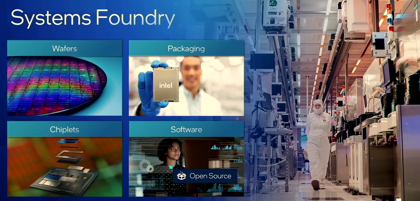
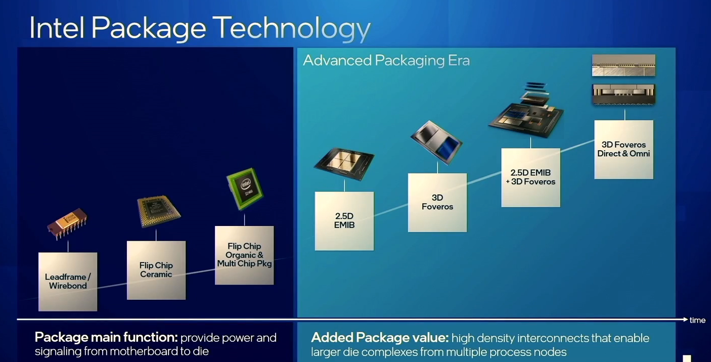
However, the idea of wafer foundry is giving way to the system foundry, with the rack becoming the system and the system a package of multiple dies and chiplets. More types of technologies are needed for 2.5 and 3D chiplet packaging, with chiplets and other IP coming together on the package to help create next-generation designs in a system foundry, which is what Gelsinger said Intel is aiming for – driving the ecosystem around these new technologies to enable designers to innovate at scale.
Unsurprisingly, Intel’s CEO sees Moore’s Law – which many industry observers see as slowing down – being foundational to all this. Gelsinger said there 100 billion transistors on packages today and that that will grow to 1 trillion by the end of the decade. He pointed to technologies like the RibbonFET transistor structure and Power VIA power delivery system unveiled last year by Intel and the use of High-NA EUV-lithography and 2.5 and 3D packaging as cutting the path toward 1 trillion transistors.
Other packaging technologies like Embedded Multi-die Interconnect Bridge (EBIM) to help tie more components together and Foveros for logic stacking will enable Intel to bring more functions into densely designed packages. New chips like “Meteor Lake” – due out next year – and after that “Arrow Lake” will take advantage of these technologies. The upcoming “Ponte Vecchio” GPU (which Gelsinger is holding in the feature image above), with its 47 active silicon tiles and more than 100 billion transistors on a single package, is as well.
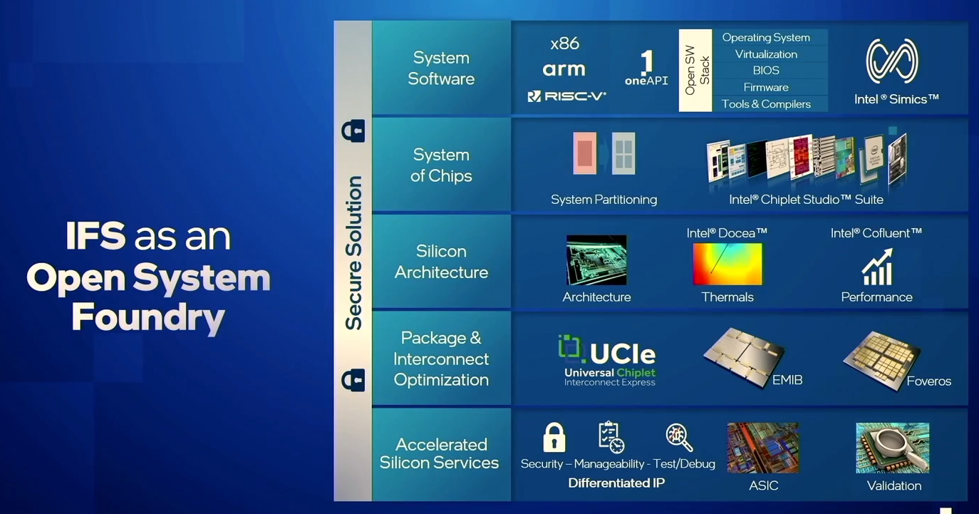
What will be important going forward is standardizing in the industry how these different pieces are put together, not only within Intel but among other industry players. A key first step was the creation earlier this year of the Universal Chiplet Interconnect Express consortium to do for chiplets what PCI-Express interconnect standard did for tying peripherals into compute systems. Chip makers are creating processors that can pull different pieces together to make them less costly to make, more adaptable to the demands of software and able to meet the growing performance and throughput demands from compute and networking systems.
Joining Intel on the UCI-Express panel are vendors like AMD, Arm, Qualcomm (which reportedly is once again eyeing the datacenter), Microsoft, Meta and Samsung, along with TSMC and, most recently, Marvell.
“Now we’re doing [what was done with PCI-Express] at the chip level and taking a monolithic system on a chip that could be constrained in die size, cost and power, and being able to disaggregate it onto a solution that takes advantage of not only the advanced packaging, but the standard mix-and-match capabilities that UCIe will enable,” Gelsinger said. “Different process technologies will be optimized for different functions – power, RF, analog, advanced logic, memory. But we also will need to tie these together in a very easy-to-use composable fashion that gives the designers the abstractions that enable them to do more complex things without the detail of each execution and hardened IP at the lowest chip level.”
Enabling all this is being able to pull together different technologies found in disparate foundries. Gelsinger sees Intel Foundry Services as an open foundry, saying Intel can bring its foundry offerings to help drive the development of chiplets in the industry, with what he called the Intel Chiplet Studio Suite of technologies to enable it across not only x86 but other architectures, such as Arm and RISC-V.
He envisions chip designers to tap into technologies from a different foundries to build processors to address their specific needs. Like PCI-Express, UCI-Express will deliver a similar level of technology interchange.
“With that, you may say, ‘I’m getting two of the chiplets from Intel, I’m getting one of the chiplets coming from a TSMC factory,” Gelsinger said. “Maybe the power supply components are coming from TI, maybe there’s an I/O component coming from GlobalFoundries.’ And, of course, Intel has the best packaging technology, so they would be the one assembling all those chiplets together into the marketplace, but maybe it’s another provider as well. We do see the mix and match. When I say the rack is becoming a system, the system is becoming an advanced chiplet based on a package, that’s exactly what we mean, how we see it evolving.”
It won’t be easy. Intel will have to create a clean separation between its product businesses – which also will take advantage of the advanced packaging technologies offered in the foundry service – and outside companies using Intel’s foundry. In addition, the consortium also includes competitors, so – like other industry groups – that will have to be navigated.
Meanwhile, Intel has its own challenges. It has plans for new fabs in Ohio and Gelsinger was a key industry driver behind the $53 billion CHIPS Act signed by President Biden earlier this year that is designed to help fund more chip making in the United States. But as we explained last month, Intel has some operational and financial problems that while not impossible to fix, they are expensive And again, it comes at a time when companies like AMD and Arm that for years had their knives out for Intel are finally drawing blood and when top public cloud providers – which are the key customers for chip and systems makers – are more than willing to go their own way in designing their own processors.



Intel has one advantage huge up its sleeve: the best single core performance in the industry. It comes at the price of power efficiency and the number of cores they can fit on a die. AMD is fighting back by using smaller cores, which provides superior power efficiency and the ability to put more cores in a CPU. That plus switching from GlobalFoundries to TSMC allows them to press that advantage even further. ARM has the best power efficiency but no one – not ARM Neoverse or its derivatives like AWS Graviton and Nvidia Grace, Apple and its M1 and M2, Nuvia, Ampere and their custom CPU etc. – have been able to match AMD’s single core performance, let alone Intel’s. Also – and I don’t know why this is spoken of so infrequently – x86 CPUs can be multithreaded where ARM is single threaded. ARM Holdings has tried to obfuscate this by replacing SMT and hyperthreading with some designs that maximize single thread performance and other designs that maximize core counts (it is impossible to do both).
So ultimately you have AMD and the various ARM competitors taking advantage of Intel’s taking 6 years to fix their 10nm node problems – and having to remain on 14nm for every CPU that had more than 4 cores in the meantime – to pass off what was primarily the benefits of being on TSMC’s 7nm and lower nodes as “beating Intel.” And they’ve had a pliant media that has been willing to adopt that storyline for various reasons, to the point where it is now common to claim that Intel is on a downward spiral from which they will not be able to extricate themselves. I don’t know which of the claims is more nonsensical. The claims that Intel is going to stop manufacturing GPUs when they already have data center and OEM buyers lined up, or that Intel is all of a sudden going to be unable to pay for their new foundries when they have never had such problems in the past.
Presuming no further delays – while they will be increasing their use of EUV, the big test will be shifting from FinFET to GAA RibbonFET in 2024 – by 2025 Intel will be on a similar process to AMD and the ARM server suppliers. (Apple will be on a more advanced one, but Apple only competes with Intel in the minds of their fans. Apple has from 5% to 8% of the PC market share and does not make server CPUs at all.) At that point things will largely return to the situation that it was before Intel’s 10nm roadblock: Intel will reap the benefits of having superior single core performance to AMD while being able to offer competitive core counts and power efficiency. ARM will retain a core count and power efficiency advantage, but much smaller than before, and further they will be limited to applications that don’t require SMT/hyperthreading i.e. cloud native applications.
While Intel will not return to their former dominance as you mentioned, AMD and ARM will never again enjoy the 7nm (AMD) and 9nm (Apple) process node gap that they did as recently as 2021. And yes, AMD and Nvidia will lose some GPU market share to Intel. Intel Foundry Services will also succeed in creating a 3 way competition between themselves, Apple and Samsung. The CHIPS act did not merely provide $50 billion to defray the cost of foundry construction – of which Intel can only claim a maximum of $3 billion in any case – but it also provides incentives for American companies to use American foundries. While Samsung, TSMC and other foreign companies can partially benefit by opening American foundries, the maximum incentives will be given to companies that use American foundries operated by American companies. While major companies like Apple, AMD, Nvidia and Qualcomm do not need those incentives, lots of smaller companies will indeed switch to IFS to take advantage. Also, despite people who are convinced otherwise, there really is nothing that prevents Nvidia and Qualcomm from shifting some of their business to IFS. They lack the status of direct competitors with a long history of enmity that Apple and AMD have with Intel. Further, Qualcomm and Nvidia prefer a multi-supplier strategy anyway. They were both relying on Samsung as their secondary supplier until Samsung’s combination of power efficiency (due to low transistor densities) and yield problems forced them to rely on TSMC exclusively. Samsung is retooling to win them back, but they won’t be able to make a play for them until 2024 at the earliest. Again, Intel’s current miserable experience with their GPU launch – which I have stated before was caused by their bad decision to choose TSMC’s 6nm node yields over Samsung’s 4nm node availability – shows that delays do happen. Apart from that, this is right about the time that Intel’s RibbonFET 20A node goes online in Ohio.
Intel isn’t “too big to fail.” Instead they offer a number of real advantages that legitimately make their products the best choice for a lot of customers.
Power has the best single core performance in the industry, and has for 21 years.
Pat is right about Intel Packaging being the best in the world, because I had put in the right building blocks in place, including some that I had originally developed at Motorola 3 miles further north on the same street in AZ. As to EMIB ( which BTW uses one of my 1991 inventions ), 6 mo.s back our “friends” in Hsinchu tried to replicate this already 6 yr old technology, that had totally invalidated the Taiwan approach using all Silicon ( expensive but their Fabless customers had no choice but to swallow the expense ), is nowhere near in terms of either electrical performance or cost, but a certain “fruity” Co. had no choice but to accept it for their Vanity 2 chip processor anyway. In order to catch up and then pull ahead in the Transistor race, Intel still needs to make major personnel changes in its TMG group ( responsible for Transistor design & process development ). This when Pat G. has been back 1 and 1/2 yrs already !