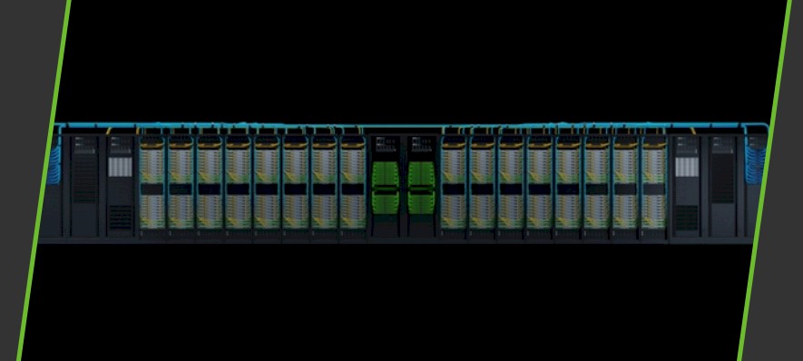
If you were hoping to get your hands on one of Nvidia’s “Grace” Arm-based CPUs, then you better be prepared to buy a pretty big machine.
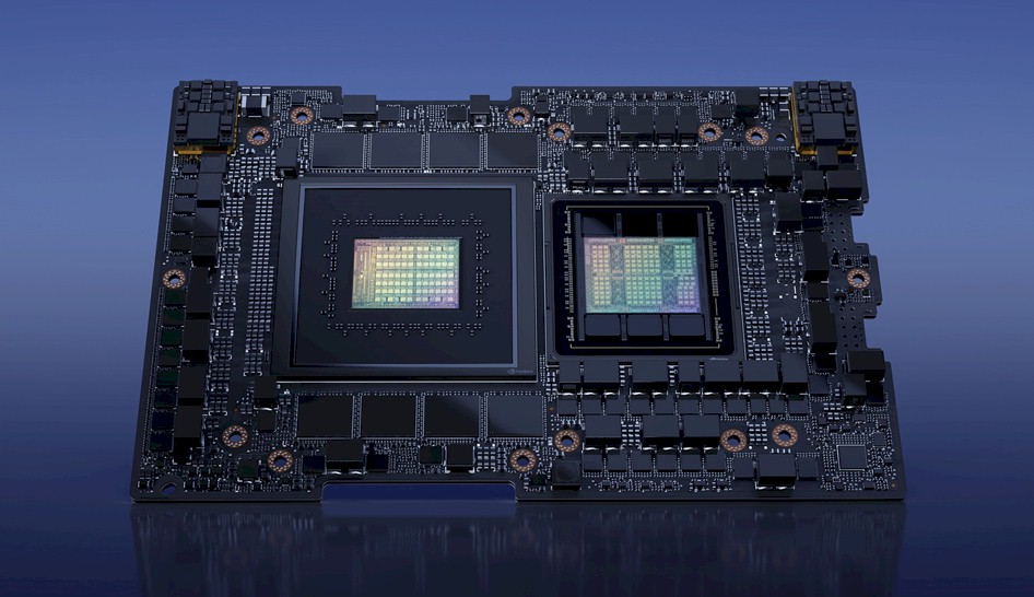
The Grace-Grace superchips, which have two CPUs on a package with NVLink 4.0 chip-to-chip (C2C) links, and the alternative Grace-Hopper GH200 superchips that weld a Grace CPU to a “Hopper” GH100 GPU accelerator, are coming out in very high end systems. But nothing, as far as we can see, that scales down to a single unit 1U or 2U rack server or even something the size of DGX-A100 or DGX-H100 system, which packs two X86 servers and eight GPU accelerators into a single 5U rack chassis, is being made available right now from Nvidia. There are reference designs called MGX that have either superchips in them, which we showed off last year, but the DGX GH200 is only available in 32, 64, 128, and 256 GPU configurations, and we suspect that the volume of shipments are going to end up in these machines and not the MGX designs at first. Demand is going to far exceed supply, and demand is going to be met on high.
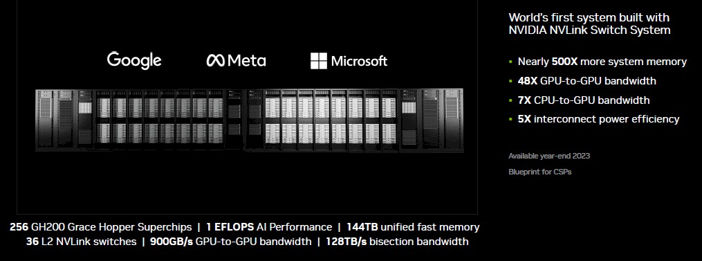
Nvidia is going big with the Grace-Grace and Grace-Hopper superchips, installing them in several supercomputers around the world as well as selling the Grace-Hopper combo in a new DGX-GH200 system that combines 256 of the Grace-Hopper superchips into a single shared memory GPU cluster that has the CPUs hanging off the GPUs providing host compute and access to the larger (but slower) main memory in that Grace host.
The general availability of the long-awaited Grace Arm CPU was announced this weekend by Nvidia co-founder and chief executive officer Jensen Huang in a keynote address at the Computex trade show that is held around this time every year in Taipei, Taiwan. (Technically it was Monday morning in Asia, but it was earlier in Europe and much earlier in North America, the latter of which in America are celebrating Memorial Day to commemorate the end of the Civil War and to toast the unofficial beginning of summer.)
Also as far as we know, the Grace CPU still does not have a product name, at least not one that has been revealed and ditto for the Grace-Grace superchip, but CG100 makes sense for a single Grace GPU given the chip maker’s GPU naming conventions – G for GPU, first initial from the product code name such as Pascal, Volta, Ampere, or Hopper, followed by 100 to denote top-end datacenter compute engine. So CPUs should start with a “C” and have a “G” for Grace and “X00” will tell you how many there. And that would make a Grace-Grace superchip “CG200” and a single standalone Grace a “CG100.” All of this will probably be a bit confusing given that “G” is also meant to designate GPU.
The Grace CPU might be shipping, but a lot of the feeds and speeds had yet to be revealed on the device as we went to press. We had been told that there were whitepapers being prepped for the Grace chip as well as the new DGX GH200 system that is not just being sold by Nvidia but is apparently going to be a reference architecture blue print upon which Google, Meta Platforms, and Microsoft are going to riff on as they build out their AI training infrastructure to handle 1 trillion parameter large language models and massive recommendation systems, which need more memory than can fit onto a GPU to store their embeddings.
Now is a good time to review what we do know about Grace before getting into the systems that employ it.
But For The Grace Of DLRM
Nvidia doesn’t enter any adjacent business in the datacenter – by either engineering a hardware and software stack or by acquiring – unless it has to. Nvidia first talked about making datacenter-class Arm CPUs with its ambitious “Project Denver” plan announced in January 2011, when Arm-based CPUs were still in their infancy in the datacenter. The Denver hybrid processors were supposed to have both beefy CPU and beefy GPU capacity and obviate the need for an X86 processor entirely as the host processor. Nvidia was rumored to be creating a custom Arm core that could emulate the crap out of an X86 chip as well as run in a very fast native mode, which if true could have caused big legal problems with Intel. All we know is that suddenly Nvidia stopped talking about Denver server chips as if the January 2011 announcement never happened.
And then, less than a decade later, after many failed attempts by others to create a server-class Arm CPU, Nvidia started working on the Grace CPU. At the time, IBM was the only CPU maker that had NVLink ports on its chips (the Power9) and for whatever reason, IBM and Nvidia did not work out a way to get the NVLink 4.0 protocol running atop the OpenCAPI ports on the Power10 chips. With DLRMs really needing a lot more memory, and large language models starting to need exponentially more memory, Nvidia correctly saw that it needed to control more of its hardware stack and needing a very fast way to add high capacity memory from a server to the high bandwidth memory on its GPU compute engines with something faster than PCI-Express – and with no vendors wanting to put NVLink SerDes on their CPUs – Nvidia really had no choice but to create a CPU itself so its GPU could have a memory accelerator and a serial processing accelerator.
And so, in April 2021, Nvidia threw its hat in the CPU ring. There are several cool things about the Grace chip. The most important thing is that it uses cheap LPDDR5 memory – the kind used in laptops – and Nvidia has enough channels on the device to provide up to 546 GB/sec of bandwidth to up to 512 GB of memory across its 32 channels. That is enough capacity to be interesting as well as enough bandwidth to be interesting for both traditional HPC simulation and modeling and for AI training for large language models and recommendation systems. That’s 8X the capacity of HBM2e memory at about a third the bandwidth at about a third the cost per GB, or about the same cost as DDR5 main memory, but with 4X the channels at one eighth the capacity but 1.5X the bandwidth. (Nvidia’s table explaining all of this was divulged in August 2022.)
From our eye, the Grace chip layout looks like it was designed to support 96 cores in a 3 nanometer 3N process from Taiwan Semiconductor Manufacturing Co and then because of issues with the 3N rollout (or to have most of the design ready for 96 cores when 3N was ready) was cut back to 84 cores and a custom 4N process (the same one used by Nvidia to make the Hopper GH100 GPU), with only 72 of those cores being promised to customers so as to improve the effective yield. Those latter numbers come from counting logic blocks on the die shots from two years ago. In a document that was given to use after the announcement, Nvidia contends that the design has 76 cores, with 72 exposed. We still think Nvidia desired to have more cores and the layout is asymmetrical, as you can clearly see in the die shot. Our point remains.
Nvidia did not use its own cores, which it could have, as we learned from Arm Holdings in September 2022, when it confirmed that Nvidia was using the “Demeter” Neoverse V2 cores created by itself. That is one generation further than the “Zeus” V1 cores that Amazon Web Services is using in its Graviton3 Arm processors. The Demeter cores hew to the Armv9-A specification and include SVE2 vector support plus nested virtualization support (important for cloud builders).
Nvidia has not announced clock speeds, but a single Grace chip has an estimated SPECint_Rate_2017 of 370, about what 36 Intel “Skylake” cores (half the number of Grace cores) would do at a reasonable clock speed. No one knows the exact width and precisions of the vector math units in the V2 core, but it looks like the performance is quite a bit higher than we expected back in August 2022.
We guessed that a Grace chip running at between 2 GHz and 2.3 GHz with a pair of 128-bit SVE2 vector math units would be able to do 2.3 teraflops to 2.65 teraflops of peak theoretical performance at FP64 precision. But if you do the math on the Isambard 3 system going into the GW4 collective in England, which has 384 Grace-Grace superchips (or 784 of the GC100 CPUs as we are calling them) and which is rated at a peak 2.7 petaflops, that works out to 3.55 teraflops per Grace chip. Like we suggested back in March 2022, we think Nvidia wanted 256-bit SVE2 vectors in its cores, or perhaps a quad of 128-bit vectors if that is what Arm Holdings is doing with the V2 cores, and if they are twice as wide then the clock speed can drop down to 1.55 GHz and hit that 3.55 teraflops per Grace number.
We shall see. (In fact, after we went to press in the middle of the night, this document became available and we can confirm it is a quad of 128-bit vectors on the V2 core, which Arm Holdings and Nvidia could have revealed a long time ago.)
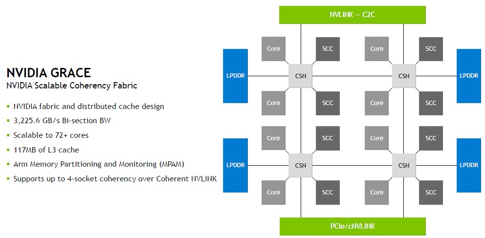
The thing that Grace is bringing to bear is bandwidth and memory coherency, both on the die and across compute complexes comprised of CPUs and GPUs.
There is a lot of bandwidth on the mesh interconnect linking the V2 cores to each other, to their scalable coherent caches (SCCs), to the LPDDR5 memory controllers, the PCI-Express/coherent NVLink bus, and the NVLink 4.0 C2C interface that links two Grace chips together:
Up to four superchips can be linked in a coherent fashion to each other, creating an eight-way CPU server with NUMA memory. That NVLink 4.0 C2C interface runs at 900 GB/sec and can hook a Grace CPU to another Grace CPU or to a Hopper GPU in a very tightly configured, coherent compute engine. Last August, Nvidia revealed that this NVLink C2C interface can move data at 1.3 picojoules per bit, which is 5X as energy efficient as a PCI-Express 5.0 interconnect and offers 7X the bandwidth of PCI-Express 5.0 x16 links. The CPUs and GPUs in the Nvidia complex have a shared virtual address space across their memories, and the GPU has access to pageable memory, memory page tables are shared across the devices, and the malloc and memap pointers used in CPU architectures can be used to access the GPU memory. And as we said before, this leads us to wonder if Nvidia will eventually offer a coreless Grace CPU as a special memory extender for those who just want to run fatter memories on their Hopper GPUs.
The CPU to CPU links (cNVLink in the diagram above) run at 600 GB/sec and more or less match the memory bandwidth of a Grace chip with a little extra to spare.
We look forward to getting more specifics on the Nvidia superchips and the systems that use them. We got a taste of possible system designs here in March 2022, and some more detailed system stats and chassis designs there in May 2022.
Enter The Dragon
Which brings us all the way to the DGX CG200 system being announced today at Computex in conjunction with the volume shipping of the Grace CPU.
The DGX H100 SuperPOD announced in March 2022 linked together 256 of the H100 GPU accelerators into a shared memory system with a two-tier NVLink Switch network that had 20 TB of HBM3 memory and 1 exaflops of AI training performance with FP8 quarter precision floating point data formats with sparsity support turned on. This DGX H100 SuperPOD system had 32 DGX H100 systems, each with eight GPUs and a pair of “Sapphire Rapids” Xeon SP processors from Intel that did not have NVLink ports and therefore could not have coherent memory with the GPUs. (Unlike the Power9 processor used in the “Summit” and “Sierra” supercomputers built for the US Department of Energy by IBM many years ago.)
With the DGX GH200, there is the full 96 GB of HBM3 memory on the Hopper H100 GPU accelerator (instead of the 80 GB of the raw H100 cards launched earlier). And while the Grace chip appears to have 512 GB of LPDDR5 physical memory (16 GB times 32 channels), only 480 GB of that is exposed. So the Grace-Hopper complex has 576 GB of total memory. Add it up, you get 256 of these Grace-Hopper units for a total of 144 TB of coherent memory on the NVLink 4.0 fabric implemented across a spine/leaf network of NVSwitch 3 ASICs, which have 900 GB/sec ports connecting the GPUs together and the CPUs that pass through to the GPUs over the NVLink C2C interconnect. Like the DGX H100 SuperPOD, this DGX GH200 system has 1 exaflops of AI training performance at FP8 precision with sparsity support enabled, but it has 7.4X more memory and is big enough to take on some hefty training and recommender workloads.
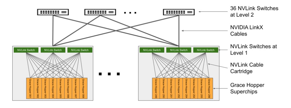
Here is how the NVLink memory fabric is implemented on the DGX GH200 system:
Each octo of Grace-Hopper superchips is cross-connected with three NVLink Switch 3 ASICs. These are effectively the leaf switches in the NVLink Switch fabric. There are 32 of these Grace-Hopper enclosures – it is not clear yet how they are physically organized – for a total of 256 Hopper GPUs and 256 Grace memory extenders that also do the host computing when needed. Level 1 of the NVLink fabric therefore has 96 NVLink Switch 3 ASICs, and these are linked to Level 2 of the fabric, which has 36 of the NVLink Switch ASICs, for a total of 132 separate ASICs.
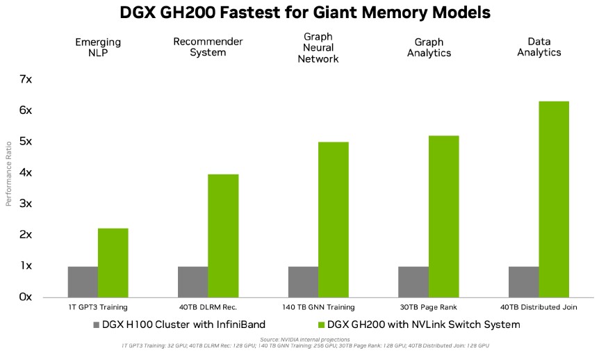
That extra memory that comes from the Grace CPUs and the NVLink fabric that makes all of the memory coherent gives substantial performance gains:
As you can see, performance ranges from anywhere from 2X to 6.5X pitting a DGX H100 cluster using InfiniBand against a DGX GH200 with the NVLink Switch fabric. Be careful with this chart, though. These are not benchmarks pitting systems with 256 GPUs against each other. These are internal Nvidia projections, not tests, and each projection is using a different number of GPUs. The 1 trillion parameter GPT3 training run is on 32 GPUs. The 40 TB DLRM test is on 128 GPUs. The 140 TB GNN training is on 256 GPUs. The 30 TB page rank test is on 128 GPUs. And the 40 TB distributed join test is on 128 GPUs.
The DGX GH200 system will be available by the end of the year, and there is no way that Nvidia or its partners are going to provide pricing for it. If you have to ask, you can’t afford it. And besides, you probably aren’t big enough to move to the front of the line like Google, Meta Platforms, and Microsoft.
We will be digging into this system and the Grace chip as data becomes available, and will cover other Nvidia announcements from Computex as well.




IDK man. Take one of the fastest compute engines on the planet and double or triple it’s performance by simply adding more memory and bandwidth and a motor to drive it? Sounds like black magic or something. 😉
Right?
The “Giant Memory Models” evaluated in the bar chart are mostly above the 20TB coherency limit of the DGX H100 with 256 GPUs (HBM3), but below the 144TB limit of the DGX GH200, and so it wins (thanks to the extra NVLink-attached LPDDR5 on Grace). It goes back to the idea of adding just NVLink-LPDDR5 to the GPU system (without extra CPU) and see how that goes I think (an idea from TNP).
Still, (to me) these units have an air of black magic to them, a thematic lovechild of Elvira and Darth Vader, a Pierre Soulages aesthetic of darkness … quite impressive (very coal stuff!).
Looks like this was published a couple of days back, imagine you’re already deep in the weeds. . .
https://developer.nvidia.com/blog/announcing-nvidia-dgx-gh200-first-100-terabyte-gpu-memory-system/
Great link! From there, one can view/download the “NVIDIA Grace Hopper Superchip Architecture whitepaper” which has more discussion of performance relative to x86-alone and x86+hopper, in different workloads. Figures 13 to 16 in that whitepaper suggest NVLink is the big boost for AI and database/hash-join, while Figs 17 and 18 show some NVLink speedup, but also some quite substantial Grace speedup for HPC/BLAS (inc. OpenFOAM motorbike). It’ll be great to compare that to MI300 … as for weeds … smoke’em if you got’em!
sorry, please delete that dumb comment
I didn’t think it was dumb at all, and it made me laugh. You’re good.
Hi, does the NVLink switch then replaces Infiniband? In the Grace Hopper white paper, it seemed like both NVLink Switch and Infiniband exist?
One is for close range NUMA-like memory sharing, the other is for ganging up pods of these.