Back in 2012, when AMD was in the process of backing out of the datacenter CPU business and did not really have its datacenter GPU act together at all, the US Department of Energy exhibited the enlightened self-interest that is a strong foundation of both economics and politics and took a chance and invested in AMD to do research in memory technologies and hybrid CPU-GPU computing at exascale. It wasn’t a lot of money, but it was enough to give AMD’s engineers a chance to think about the future on Uncle Sam’s nickel and plant the seeds for its current – and formidable – CPU and GPU business.
Here we are, more than a decade later, on the cusp of the “El Capitan” supercomputer at Lawrence Livermore National Laboratory being fired up as the most powerful (known) supercomputer in the world, using the culmination of all of that hard architectural and packaging work embodied in the “Antares” Instinct MI300A compute engine.
How did we get here? One step at a time, which is illustrated in a paper recently published by the key researchers that took AMD from nowhere to Antares. Gabriel Loh, one of those AMD techies, posted the paper in his personal archive, which was presented at the International Symposium on Computer Architecture (ISCA) in Buenos Aires, Argentina in early July. We have just come across this paper, called Realizing the AMD Exascale Heterogeneous Processor Vision, because we were on holiday that week and didn’t see it. We found the paper fun and interesting, and thought, this being summer, you might like it, too.
AMD published a similar paper last year at ISCA 2023, called A Research Retrospective on AMD’s Exascale Computing Journey, with dozens of researchers talking about how the FastForward and DesignForward work evolved towards the “Frontier” supercomputer that predates and anticipates the MI300A and El Capitan.
This story brings these two papers together for your amusement.
In The Beginning Was HSA
It is hard to remember just how far AMD had fallen out of favor in the datacenter when the funding for the DOE’s DesignForward and FastForward contracts had been awarded, and AMD would no doubt like for people like us to stop talking about it. But we believe in redemption and compassion, and this is how AMD is now at least something of a counterweight to the hegemony of Nvidia in GPUs and has absolutely taken the mantel of CPU computing away from Intel. We believe in competition, too. It has a way of focusing everyone in the game and driving innovation and progress.
The FastForward 1 program had $62.4 million in funding, and its follow-on FastForward 2 program had just shy of $100 million in funding. DesignForward had $25.4 million in funding for its first phase and we can’t find any documentation for phase two. AMD had a fairly large chunk of dough from these four investments by the DOE, and focused on heterogenous compute, processing in memory, and cache memory under FastFoward 1, and low voltage logic and new memory interfaces in FastForward 2. The DesignForward project had two phases as well, and had participants focusing on interconnects and protocols for exascale systems and then system design and integration. (There is an excellent overview of these efforts here.)
In 2015, there was a similar program with a lot more money thrown at it called PathForward, which started doing development, rather than research, for exascale-class systems. This one paired $258 million in investments across Intel, Nvidia, Cray, IBM, AMD, and Hewlett Packard Enterprise, with matching funding from these vendors that took the total investment to $450 million.
All told, there was at least $637.8 million shelled out eight years to come up with exascale hardware designs. And for the most part, the AMD plus Cray plus HPE team has won at least for exascale machinery funded in the United States. There is some pretty big iron installed in Europe that uses the same architecture, although the EuroHPC Joint Venture is hedging its bets with homegrown CPUs, accelerators, and interconnects.
Every project starts out with ideas and pretty pictures, and the future that AMD was aspiring to more than a decade ago started out with this one, which is now in the paper written by the thirteen AMD techies, many of them who became familiar names in the HPC and AI sectors because of their work on what AMD used to call Accelerated Processing Units, embodying what was called the Heterogeneous Systems Architecture back in the beginning. This image is from 2012, and comes from the FastForward 1 program:
And here is a drilldown on the first iteration of what AMD called the Exascale Heterogeneous Processor from that same time:
This EHP-1 design was really a four core design with four 256-bit vectors paired with a GPU complex with a pair of streaming multiprocessors with 6 teraflops of 64-bit vector math oomph each. Presumably this chip design supported FP32 formats, too, but probably nothing of lower precision. Remember, this was focused on HPC workloads, and transformer AI workloads had not exploded onto the scene as we now know them. AI workloads are statistical in nature, and they can sacrifice some precision for the sake of throughput and still converge to the right answer. HPC workloads are more deterministic (well, at least as far as can be said with 64 bits of data and a good algorithm) and more precision always yields a better answer. We live in an era where we are trying to make do with less precision in new HPC applications, and it may yet play out, despite the heresy this sounds like.
By 2014, AMD had figured out that the normalized cost price per unit area of chippery was going to go up by a factor of 2.5X between the 14/16 nanometer generation to the 5 nanometer generation, and that is when it switched from monolithic processor and GPU complexes to chiplet designs.
At this point, AMD also started to question the economic and technical viability of processor in memory (PIM) approaches, which the DOE had paid it to research, and also the use of NVRAM in the compute engines. AMD also was point blank about being overly optimistic about how many DRAM chips could be stacked to make HBM memory banks. The illustration above shows 16 dies stacked up, and until next year, when 12 die stacks will become commercially viable, we have been stuck at eight die stacks.
You will also not that EHP v2 has the DRAM memory stacked up above the GPU chiplets, which is ambitious indeed.
In 2016, AMD went back to the drawing board and adapted the EHP design with a third iteration:
Now, the GPU chiplets are busted in half and have eight-high HBM stacks on top of the GPUs, while the CPU chiplets are in the center of the compute engine and presumably had access to that HBM memory. This EHP v3 design made use of an active interposer underneath the GPUs, which means they have active components like routers or repeaters, instead of the metal wires that are the only thing in a passive interposer.
AMD eventually figured active interposers and 3D stacking of memory on top of compute on top of this active interposer would not be economically feasible. Which leads to the EHP v4 design in 2018:
With the first three iterations of the EHP design, AMD was trying to cram everything within the confines of its Epyc SP3 server socket. With the PathForward work, AMD stopped thinking in terms of sockets and instead thought at a system board level and figured out how to stitch a much bigger “socket” together over a motherboard using Infinity Fabric links. AMD had its own packaging designs for the GPU sockets and was keeping a close watch on the OCP Accelerator Module (OAM) socket that was created by Microsoft and Meta Platforms and adopted as an OCP standard in 2019. (AMD obviously knew about it ahead of time, and its Instinct GPUs adopt this socket to this day.)
A lot has been made of the fact that AMD chose a 1:4 ratio between CPU compute and GPU compute when it designed the actual compute engine complex for the Frontier supercomputer installed at Oak Ridge National Laboratory, but once again both of these AMD papers show, as have other schematics we have walked you through, that this is really a 1:1 pairing of one eight-core chiplet block to one GPU chiplet block, with eight of those pairs per node. See:
The Frontier node is a virtual APU, in a sense, and it is programmed as such. There are fatter Infinity Fabric pipes between the GPUs so they can share data fast and fat, with GPU chiplet pairs being very tightly coupled, and with adjacent GPU complexes connected to each other with slightly less fat and fast Infinity Fabric pipes and the CPU to GPU links being a little bit more skinny than even that.
Close, but no cigar, but Uncle Sam needed an exascale system and you do what you gotta do.
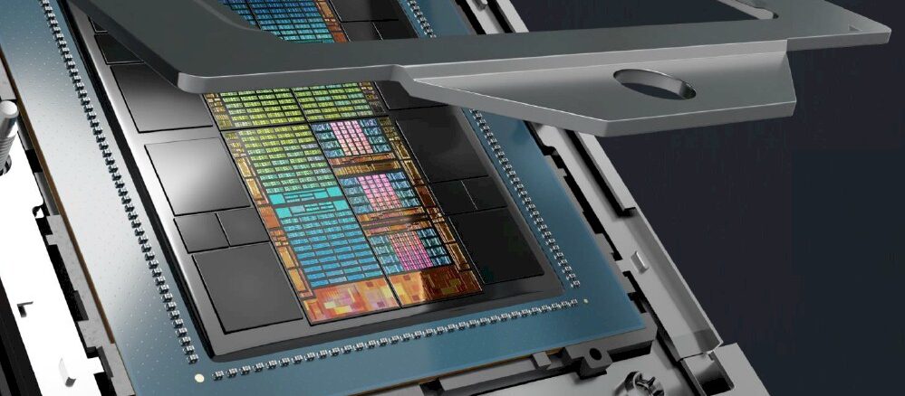
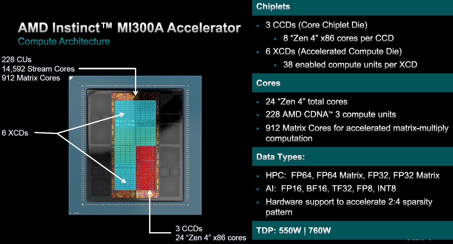
And with El Capitan’s Instinct MI300A, which was announced in December last year, AMD has done what it has always wanted to do: Create a true APU. The company has also created what is arguably the most complex compute engine socket in history. Here are the feeds and speeds:
And here is the cross section of the complex:
That is quite a silicon and metal sandwich, isn’t it?
While we admire all of the hardware advances, here is what it really comes down to. Because the CPU and GPU are truly unified, the code is not that different from using CPU-only architectures, and the second paper highlighting the MI300A gave a case in point showing data movement and synchronization for different scenarios. Take a look:
The MI300A architecture is designed to tightly couple for CPU-GPU complexes together and to use PCI-Express ports on the Epyc CPU CCDs on the complex to reach the outside world, like this:
What we want to know is whether companies will want to buy MI300A servers or use discrete Epyc CPUs paired to the discrete MI300X GPUs also in the Antares family. It will come down to price, availability, and the CPU-GPU compute ratio that companies need. What we want to know is how MI300A compares in terms of price, price/performance, and thermals with a Grace-Hopper or Grace-Blackwell discrete CPU and GPU pairing from Nvidia.
So far, we don’t have much data to do such a comparison. But we will keep an eye out.


> What we want to know is whether companies will want to buy MI300A servers or use discrete Epyc CPUs paired to the discrete MI300X GPUs also in the Antares family
Not sure about companies, but, for myself, a workstation based on one of these (I’d prefer six CPU chiplets and four GPU ones, AMD) would be perfect.
I agree as well! And Ricardo, it is so good to see you here in the comments. We appreciate you, and I can tell you that now.
All I want for Christmas is a single socket Mi300A system in a uATX form factor that I can use in a SOHO setup. Just need a couple USB4 jacks and a suite of x4/x4/x8 PCIe5 slots for ext GPU and/or IB card and/or NVMe breakout board(s). IDK if the 300A will be a historical one-off, but I hope it will not be. Seems to me the 300A’s heterogeneity is AMD’s answer to CUDA: any damn fool C++ programmer should be able to exploit GPU compute with this product. For example, it actually has enormous applicability to gaming and also graphics & video production if one can see past the HPC/AI targetting. AMD should make a version of 300A with a strong graphics output subsystem or perhaps just use RDNA, it would be an absolute top gaming / professional platform. It could possibly blow nVidia right out of the consumer market because of it’s ease of programming.
I agree. I want a PC made of this.
Isn’t that what Strix Halo is going to be? An APU with 16 Zen5 cores with 40 CU of RDNA 3.5 giving an iGPU that’s about a 4070 equivalent with say 128GB fast DDR5 unified shared memory?
I don’t think Halo will have the CPU and GPU talking to the same RAM using the very same pointers.
“So far, we don’t have much data to do such a comparison”
Isn’t that question being a thorn all along on AMD’s side? Where are the benchmarks? Why not run MLPerf and publish what you see. I mean they seem to be proud of what they are doing. So, why hide the results?
I will taunt them a bit….
There is only one reason AMD isn’t participating in industry benchmarks, and no taunting will help: the results don’t show well. Some startups have complained about the costs to participate in MLPerf. Cerebras concluded it wasn’t worth the resources which one can understand for a cash strapped startup. AMD at this point can’t make a similar claim, they’ve got plenty of resources, and there is no way they are not running these benchmarks internally. It’s also odd because their customers (and potential customers) also run that data on AMD chips as part of their evaluations. And they are still buying apparently. So effectively the only perception AMD are managing by holding back on MLPerf is the public’s. But the public by and large, aren’t customers for these type of chips.
>>And they are still buying apparently
that claim doesn’t seem to be valid either based on past four quarterly reports. AI scaling is a nasty problem. The narrative that it is a chip problem and hence we can beat Nvidia with a bit more memory or some other clever trick kind of propaganda is the root of all these problems.
Superb article … perferct for this relaxing summer evening (it made my Thursday)!
“So far, we don’t have much data to do such a comparison. ”
AMD had a one rack entry of their El Capitan nodes in the top500 list … 19.65 petaFLOPs.
https://www.llnl.gov/article/51231/llnls-el-capitan-debuted-new-top500-list-worlds-most-powerful-supercomputers
“one computing rack each from El Capitan’s “Early Delivery System” (EDS), LLNL’s newest unclassified supercomputer RZAdams and its unclassified “sister” system Tuolumne. All three registered 19.65 petaFLOPs (nearly 20 quadrillion floating point calculations per second) on the High Performance Linpack (HPL) benchmark used by the Top500 organization to determine the world’s fastest supercomputers. “