
Like many a decade ago, we were enthusiastic about the prospect of triple-hybrid systems in the datacenter. We were convinced that there was a place for CPUs, for GPUs, and for FPGAs in complex and high performance systems because each of these devices were really good at different things and because most application workflows had elements that fell cleaning into serial and parallel processing that was either relatively static or changing all the time.
When the code is changing all of the time, then the programmability of the CPU and the GPU becomes most important, and a lot of applications are coded in C, C++, Java, Python, Fortran, and a few other languages and either run close to the iron or within a kind of virtual machine that abstracts the underlying hardware and is interpreted on the fly. CPUs are used for serial work, where getting an answer fast usually means running on a fast core, and for algorithms that are numerically intensive and are doing a lot of multiplication and addition, you offload this to a GPU, whose parallel processing capabilities are generally an order of magnitude higher than the CPU.
The FPGA fit into this triple-hybrid system where high performance for calculation or data manipulation was important, but the algorithms of a workload did not change much – maybe every couple of years, maybe a few times a year – instead of daily or weekly as happens in many industries. An FPGA could do certain work a lot faster than a CPU, but it was never as power efficient and it certainly was not less expensive, but it could deliver better bang for the buck and a lot more bang for certain kinds of dataflow work. (An FPGA is malleable dataflow engine, even if it does increasingly have hard-coded components like Arm cores, DSP blocks, and SerDes communications.
Perhaps more significantly, sometimes you need higher performance than an algorithm written in C++ or Java for a CPU, but you do not need a chip in such high volumes that it justifies making a full-blown custom ASIC. This happens in telecom and networking systems all the time. This is distinct from the prototyping that happens on FPGAs – often banks of FPGAs – to create a model of an ASIC so it can be tested, which is another important use of FPGAs. We think of that as ASIC prototyping, and what we are referring to above is used in production inside of a switch or some other kind of gear; it is not prototyping, but more of a half-way point between a generic CPU algorithm and a full-blown custom ASIC.
When Intel shelled out $16.7 billion in June 2015 to acquire Altera, one of the ideas is that the DPU, as we now call it, would be that same kind of application/device (it’s an arbitrary line) that we are talking about that needs speed, you will pay a premium for it, and will run better on an FPGA than on a generic CPU. And someone got it inside of Intel’s head that a third of all hyperscale and cloud servers would have one of these on-bus, in-system FPGA accelerators. And it did the math for server shipments in a decade and realized that all of those functions would move off CPUs and it better have a device to catch those customers. Cha-ching! Altera shareholders cash out, and Intel buys in to FPGAs.
Part of the thinking was also that many of the HPC and AI algorithms that were being offloaded to GPUs could be moved onto FPGAs. At the time, AMD didn’t really have a datacenter GPU offering that was competitive with the Nvidia lineup, but it was better off than Intel, which only had GPUs on laptop and entry server chips. Still, given AMD’s desire to have more domain expertise for accelerated compute and its FOMO for the FPGA wave, it was no surprise to us or you or Wall Street that AMD wanted to buy rival FPGA maker Xilinx in October 2020, a deal it completed in February 2022 for nearly $49 billion.
Since then, Intel’s datacenter GPU business has fizzled and AMD’s is finally getting traction as it has delivered competitive hardware. And both companies believe that there is a place for FPGAs in the world and in the datacenter, but perhaps cooler heads have prevailed.
Sandra Rivera, who used to run Intel’s Data Center & AI business unit and who has been tapped to be chief executive officer in charge of the arm’s length and reconstituted Altera, hosted the Altera Innovators Day this week, and at a prebriefing we had a chance to talk about FPGAs in the datacenter and what the opportunity was looking forward – particularly in light of the fact that the hyperscalers and cloud builders by and large did not do what they said with FPGAs being used for accelerators and the central compute engines for DPUs. We are going to quote Rivera in full because the answer is complex because the question is:
“If you look at the thesis for the acquisition of Altera into Intel, so much of it was built around the opportunity for datacenter and enterprise, whether that was cloud or enterprise infrastructure and also communication service provider networks, both the radio access network and the wireless network, but as well as the centralized core, which is a lot of datacenters. And I will say that we actually did a very good job of fulfilling the thesis for what we thought we could go after and what we could win from the standpoint of the emergence of the IPU socket, which was one that that we probably didn’t see in 2015 but we saw increasingly as the decade moved on. And more of the cloud service providers wanted to do offload so that they can sell the cores on a CPU. Then everything having to do with storage acceleration or just overhead management of the platform, they wanted to offload. And we actually won every single socket that was available in the market for an FPGA. There were a couple sockets that were dedicated to ASICs. Of course you are familiar with AWS Nitro, but Intel actually won another big one with Google and the ‘Mount Evans’ platform. But every single other IPU socket, Altera, then PSG, but now Altera, won. So we did very, very well there.”
“We also did well from a communication service provider perspective when we went through the whole 5G transition and we won many of the platforms from what we call the TEMs, the telecom equipment manufacturers, that were out to bid. We won a lot of those sockets as well, not just in Europe and in the United States, but in China. Now, some of that has been obviously constrained due to export controls, but we had won a lot of those.”
“Where we did fall short is in thinking that we could do more of that co-packaging of the FPGA with the CPU. as an example, because we didn’t realize, I think at that point, how much you would be constraining one device or the other device, where the customers really want to use both devices at their full potential. And so that value proposition was never realized, and we moved away from that strategy within the first couple of years. And then the other area, which is so different for us now that we are standalone and that we are driving an FPGA strategy as an FPGA company, is that that midrange, that more low-end, power-constrained, cost-constrained environment and segments were not as important to us driving an Intel CPU first strategy.”
“And we weren’t, as I would say, invested in building out the distribution network and all of the capabilities that, of course, now we are completely focused on in terms of reference kits and getting more reach and scale out of the portfolio through our partners. And that’s because, from an Intel strategy perspective, it is less important than the top 25 customers that make up most of Intel’s revenue. So there were some learnings clearly along the way. We did some adjustments. We did quite well where we were focused. We did not do as well where we just weren’t paying as much time and attention. And you know, that’s the thing that we get to change now, because this is all we do and we are committed to the entire breadth of use cases, applications, market segments, and capabilities in the portfolio.”
That is a history and interpretation that we would not argue with, but we pressed further for a more specific answer about the future of FPGAs in the datacenter, and quipped that the FPGA opportunity in the datacenter now is less than we thought it would be here and now a decade ago, but no less than it has been in the past several years. To which Rivera responded:
“It’s a huge opportunity. The thing is that in that part of the market, the reason it’s so important to stay engaged on datacenter, and certainly with cloud service providers and communication service providers, is that the technology transitions happen there. So that’s where you get new memory technologies. That’s where you PCI-Express Gen 6.0 and 7.0 show up first. That’s where AI is driving so much innovation. That’s where you need more networking and transceiver capability. That’s where you need interconnects like UCI-Express and CXL capabilities and, particularly, where we have actually been winning quite a lot lately in test and measurement. They need that first, because as those devices come out from the product development organizations, you need to be able to test them. And so the test and measurement industry is typically tip of the spear.”
“But what you will also see is that some of those IPU sockets, or some of those AI NICs, eventually go to ASICs because the volumes are so high and gets you over that crossover point. That probably will be true for a handful of customers, a handful of companies that have that capability, given how expensive ASICs are to develop, particularly on new process technology and the complexity of packaging and process nodes, but there’s always this refresh of new devices that are moving to ASIC. What are the other opportunities that we go after with an FPGA, which is always the place where you trial and pilot and in many cases, deployed for many years, and in other cases, it’s more transitory in terms of when you can make that business case to move to an ASIC.”
The job that Rivera has ahead of her is daunting, but someone has to do it, and it is important to remember that Altera and Xilinx have a long history of leapfrogging each other in programmable logic device. Here is the business roadmap:

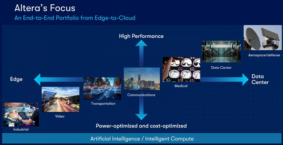
The business roadmap is driven by the product roadmap, and the arm’s length Altera is on schedule for production of its Agilex 3 FPGA in the middle of 2025, rounding out the current Agilex 3, Agilex 7, and Agilex 9 devices already launched.
The Agilex 3 is a small form factor FPGA with a pair of Arm Cortex-A55 cores and between 25,000 and 135,000 LookUp Tables (LUTs) of programmable logic capacity. The Agilex 3s may end up in some datacenter devices, but they are really aimed at edge, vision processing, and factory automation workloads that need some AI acceleration and auxiliary compute. Importantly, the Agilex 3 devices have1.8X the performance of the relatively old Cyclone V devices they replace.
This may not be exciting to the datacenter crowd, but distributors of FPGA boards account for 80 percent of the unit volume and 50 percent of the revenues for Altera, and with the reconstituted Altera re-engaging with its channels, this product is aimed squarely at them and therefore at getting the Altera business back on track. Just like PC chips paid for Intel’s expansion into the datacenter, the Agilex 3 can create the revenues and profits that allow Altera to invest on the kind of FPGA devices that datacenter customers might choose for workloads (or portions of them) that are not as well suited for CPUs and GPUs.
For a long time, we thought that Intel was going to push FPGAs into datacenters aggressively and become a creator and seller of pre-configured FPGA “software” that it would sell on its PAC, short for PCI-Express Accelerator Card. Rivera put the kibosh on Altera making cards and selling them and will leave that to its partner channel.
The thing that is in the favor of FPGAs and the mitigates against the massive migration to ASICs is the increasing cost of developing for each process node, and she rattled them off using Taiwan Semiconductor Manufacturing Co as the example, which was fun: $40 million for a 28 nanometer device, 100 million for a 14 nanometer device, $300 million to $400 million for an N7 device, $600 million for an N3 device, and $800 million for an N2 device. What this means is that the volume crossover to be able to afford developing a custom ASIC is absolutely huge. And while Rivera concedes that an FPGA is not going to replace a GPU for large scale AI training – and no one was expecting that anyway – there are opportunities for FPGAs in AI pre-processing and post-processing in training, AI inference, 6G wireless flatforms, and security processing.
That might be much less exciting than many of us wanted, but it is the truth. And we can work with that. And do can Wall Street as Intel tries to take Altera public around 2026 or so, raising capital to bolster its foundry business.

Bookkeeping Helps Intel Recover From Server Recession A Little
Accounting is something of an art, and companies always save some accounting tricks – perfectly legitimate items that meet the discerning eye of financial standards – to goose their numbers when they really need it. When they really need to tell a turnaround story. And so it is with Intel …

Talking Servers With Inspur And Intel
Any time a server maker comes into the global market and bypasses Cisco Systems, Lenovo, and IBM to become the third largest seller of machines in the world, you should pay attention. This is precisely what Inspur Information, the server unit of Chinese IT supplier Inspur Group, has accomplished, and …
Intel’s Datacenter Decline Not As Bad As Expected
Incoming chief executive officer and long-time Intel employee Pat Gelsinger is talking the helm of a chip company that has plenty of issues to sort out, but there is some good news as Intel reports its financial results for the fourth quarter of 2020 and Gelsinger gets ready to take …
Be the first to comment