
If you want to be a leading in supplying AI models and AI applications, as well as AI infrastructure to run it, to the world, it is also helpful to have a business that needs a lot of AI that can underwrite the development of homegrown infrastructure that can be sold side-by-side with the standard in the industry.
That standard is, of course, the MGX, HGX, and DGX platforms created by Nvidia, which use its current “Hopper” and “Blackwell” GPU accelerators and related NVLink and NVSwitch, Quantum-X InfiniBand, and Spectrum-X interconnects. But as Nvidia’s deep profit pools show, this is not the cheapest platform to acquire even if it is arguably the best and most complete AI platform yet developed.
Google is no slouch when it comes to creating AI platforms, which is why it developed its Tensor Processing Units, or TPUs, more than a decade ago and why it also started exposing them to the outside world as a rentable commodity seven years ago on Google Cloud. Today, at the Next 2025 conference in Las Vegas, the search engine, advertising, and media conglomerate that is also one of the heavy hitters in developing AI models and embedding AI functionality into applications unveiled the seventh generation of its TPUs, code-named “Ironwood” and presumably to be called the TPU v7p.
We are grateful for the synonym that is enabled by the use of a code-name, but Google could also have confirmed that it will be called the TPU v7p when it ships sometime later this year. We reckon it will be towards the end of the year, perhaps in the fall and maybe even in the early winter depending on how tough the manufacturing ramp is.
Amin Vahdat, vice president and general manager of machine learning, systems, and cloud AI at the company, walked through some of the specifications of the Ironwood chip in a prebriefing ahead of the Next 2025 event and during the opening keynote today. As usual, we have to piece together the data from across the blogs and comments, and make our own guesses about certain salient characteristics of the Ironwood chip, much as we had to do a year ago with the “Trillium” TPU v6e chip.
Google eventually gets around providing details on each generation of TPUs when they become generally available, and did so with the Trillium chip sometime earlier this year, which we have discovered. We expect it will do the same for the Ironwood chip when it ships later this year. If you see it before we do, pipe up.
The Ironwood TPU is by far the biggest and baddest AI compute engine that Google has ever created, and it is also put in to the most expansive “hypercomputer” cluster configurations that Google has ever assembled. The Ironwood chips and systems are also flexible. First of all, they are designed to run both AI training and AI inference workloads, and particularly the mixture of experts (MoE) chain of thought reasoning models that are heavy on the inference but that give much better answers to questions than do the frontier models that were popular a year or two ago.
The TPU v7p chip is the first TPU that supports FP8 calculations in its tensor cores and matrix math units. Prior TPUs supported the INT8 format and processing for inference and the BF16 format and processing for training. The Ironwood chip also has a third generation of the SparseCore accelerators that first debuted in the TPU v5p and were enhanced with last year’s Trillium chip. The SparseCore chips were initially designed to accelerate recommendation models that make use of embeddings to make recommendations across classes of users. The third generation SparseCores in the Ironwood chip have various algorithms encoded in them to accelerate financial and scientific calculations, but the specifics of this were not revealed.
Here is the ship that Vahdat showed off on stage, and it is interesting that he did not hold it up and therefore give us a sense of its relative size:

That’s not a very good chip shot, but if we zoom in on this one that Google have us, we can see the two compute chiplets:
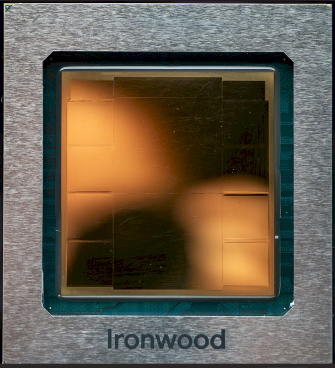
As you can see if you squint, there are two chiplets in the center of the Ironwood package, which leads us to believe that this is not a monolithic chip like previous TPUs. To our eye, the combination of chips looks a little bit bigger than the reticle limit. There are eight banks of HBM memory, four on each side and presumably HBM3E if it is shipping this year. That means each stack is eight DRAM high at 3 GB apiece, for 24 GB per stack.
The Iron word package includes a central chiplet above the compute dies and another two chiplets above the memory banks along the top edge as well. These are no doubt I/O dies for the inter-chip interconnect (ICI) that Google uses to electrically link TPU chips into pods. Larger aggregations of TPUs are further lashed together with Google’s “Jupiter” optical circuit switches.
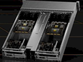
Here is what an Ironwood board looks like:

Like previous TPU designs, there are four Ironwood TPUs on a system board. We are trying to get to the bottom of what all of that chippery is on the board. It looks to us like the TPU system board plugs into a backplane, and there are probably two of these in a host server as well as the host CPU, which could be one of Google’s own Axion Arm server CPUs these days. There are network interfaces for linking the TPUs to each other in the pod.
The Ironwood TPUs are podded up in two different configurations: a 256 compute engine pod suitable for inference, and a 9,216 compute engine pod suitable for training. (If you had a very large inference job, we suppose it could run on the bigger pod.) The TPU pods employ the ICI in a 2D or 3D torus configuration, depending on the scale. Here are how the prior two generations of TPU pods that employ the more scalable 3D torus topology to the forthcoming Ironwood pod look like:

With the Ironwood TPU v7p, the pod size has increased by 2.85 percent compared to the prior TPU v5p pods, which isn’t all that much but hey, take it. At the same BF16 resolution, AI training performance for the TPU v7p chip has increased by 5X over the TPU v5p and so has inference performance using either INT8 or FP8 data types. (We are not sure that there is an INT8 data type, but we presume that there is for backwards compatibility.) For AI training, the FP8 data type allows for training throughput to be doubled and therefore is 10X higher than the BF16 used in the TPU v5p. The HBM memory capacity is 2X higher on the Ironwood package, and memory bandwidth is 2.7X higher, too.
The ICI interconnect bandwidth is 12 percent higher on the new chip, and on a third fewer links, with the TPU v7p having four ICI links running at 1.34 Tb/sec and the TPU v5p having six ports running at 800 Gb/sec.
Here is a more complete TPU salient characteristics table we have put together, filling in blanks as best as we can:

We have done our best to estimate missing data, which is shown in bold red italics. We have also gone back into the TPU manuals and updated the Trillium TPU v6e data where we could find it. By the way, Google is making lots of comparisons to Trillium, which is fine for AI inference, but if you are comparing for AI training, then the TPU v5p is the better benchmark notch.

For AI training, here is what matters. The TPU v5p pod with 8,960 compute engines topped out at 8.22 exaflops at INT8 resolution for inference and half that or 4.11 exaflops at BF16 resolution for training. The biggest Ironwood pod with 9,216 compute engines will have 42.52 exaflops at FP8 (and possibly at INT8) and 21.26 exaflops at BF16 for training. That’s a factor of 5.17X more oomph in a single system image. And with OCS switching, Google could lash together 100,000 TPU v7p compute engines in a single datacenter, as it has done with the Trillium TPU v6e devices already.
We have no idea what Google might charge for Ironwood capacity. But you can bet we will let you know as soon as we do. The pricing and relative bang for the buck shown above was current last summer.
This chart below was useful in allowing us to calculate the watts used by the more recent TPUs, which Google did not provide:

Google likes to make comparisons to the TPU v2, which was the first of its homegrown AI engines that could do both training and inference and which was announced way back in May 2017. Capacity based on the TPU v2 was available for rent in the third quarter of that year. Google, of course, does not sell TPUs themselves or systems based on them, and it doesn’t allow third parties to do so, either.
A factor of 3,600X increase in performance and a factor of 29.3X improvement in performance per watt seems impressive, and all that performance in the big bad Ironwood pod burning 10 megawatts seems reasonable. But we have to do some research to figure out how that compares to Nvidia systems. (It depends on what you call an accelerator memory domain and what you don’t.)
We would love to know how much TPU capacity Google has installed, what the plan is for both Trillium and Ironwood installations, and how much is allocated for Google’s own internal use and how much for cloud users. We will ask.

Cerebras Shows Off Scale Up AI Performance For Big Pharma And Big Oil
Historically, the largest organizations in the world – the Global 2000 plus the biggest national government and academic research institutions – have always had the most complex data processing needs. And by virtue of the size of their IT budgets and the sophistication and scale of their workloads, they get …

Nvidia Entangled in Quantum Simulators
Quantum simulators are a strange breed of systems for purposes that might seem a bit nebulous from the outset. These are often HPC clusters with fast interconnects and powerful server processors (although not usually equipped with accelerators) that run a literal simulation of how various quantum circuits function for design …
MGX: Nvidia Standardizes Multi-Generation Server Designs
Updated With More MGX Specs: Whenever a compute engine maker also does motherboards as well as system designs, those companies that make motherboards (there are dozens who do) and create system designs (the original design manufacturers and the original – get a little bit nervous as well as a bit …
Do the Ironwood tensor cores support FP32?
Both the compute chiplets in Ironwood and Blackwell are rectangular but Ironwood’s compute chiplets are closer to a square than Blackwell. In both cases, the short sides are next to the HBMs. The percent of the short side next to HBM is bigger for Ironwood than Blackwell because there is some space between the HBMs on Blackwell Ultra but not Ironwood. This suggests the Ironwood compute chiplets are smaller than Blackwell, assuming the HBM for both are the same size.
It looks like Ironwood is not using Micron’s HBM3E, at least not exclusively, because Micron’s HBM3E has a bandwidth of 1.2 TBytes/sec per stack and capacity of up to 36 GBytes per stack.
The DC-to-DC converters below the Ironwood chips can be identified by being next to round decoupling capacitors. Based on the heatsink fins on the DC-to-DC converters, it looks like the system board is not completely liquid cooled or maybe not liquid cooled at all.
NVIDIA’s Hopper and Blackwell chips have two FP8 formats: E4M3 (sign bit, 4 exponent bits, 3 mantissa bits) and E5M2 (sign bit, 5 exponent bits, 2 mantissa bits). E4M3 is used for weights and forward activations. E5M2 is used for gradients. I wonder if Ironwood supports both of these FP8 formats. DeepSeek V3 only uses E4M3.