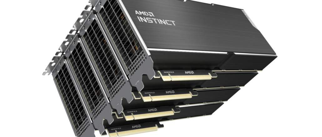
It is hard enough to chase one competitor. Imagine how hard it is to chase two different ones in different but complementary markets while at the same time those two competitors are thinking about fighting each other in those two different markets and thus bringing even more intense competitive pressure on both fronts.
Welcome to being AMD. Just as AMD has gotten two generations of its Epyc processors out the door to compete well against Intel’s Xeon SPs and is readying a third generation (in this case the “Milan” Epyc 7003s that will ship later this year for revenue and be launched formally in early 2021) to pull considerably ahead, and just as it has gotten two generations of its Instinct GPUs out the door – the Instinct MI25 in 2017 and the Instinct MI50 in 2018 – and is now at the SC20 supercomputing conference unveiling the Instinct MI100, Intel is preparing to enter the market with its “Ponte Vecchio” Xe HPC next year as AMD looks to compete pretty well against Nvidia’s current “Ampere” A100 GPU compute engine, and Nvidia is in the process of buying Arm Holdings for $40 billion to try to drive Arm server chips into the datacenter against AMD Epycs and Intel Xeons.
But at the moment, if the upper echelon of the HPC market is any kind of leading indicator – and we definitely believe that it is – then AMD is doing a remarkable job setting itself up to take share away from Intel in CPUs and Nvidia in GPU accelerators. The Instinct MI100 GPU accelerator that AMD is announcing today as the SC20 supercomputing conference is in full swing is the first step in revealing how this has been done, and therefore, where at least some of the HPC and AI market will be heading in the coming years.
Unlike CPUs and FPGAs, where there seem to be endless variants of features turned on or off to provide a SKU stack, this does not happen much for HPC and AI compute engines based on GPUs. Nvidia has two variants of the A100 – one that speaks NVLink 3.0 and one that speaks PCI-Express 4.0 – and the “Arcturus” GPU at the heart of the Instinct MI100 (Radeon is no longer part of the server accelerator brand) has precisely one SKU. There is a chance that it may have two if all of the compute elements inherent in the die are able to be activate as yields improve on the 7 nanometer process from Taiwan Semiconductor Manufacturing Corp used to make the Arcturus chip improve. But we wouldn’t count on it.
This certainly did not happen in the last generation of Instinct GPU accelerators, which came out two years using the “Vega 20” GPUs based on its Graphics Core Next (GCN) architecture clocking at 1.8 GHz. The top-bin Instinct MI60 had 64 compute elements with a total of 4,096 stream processors while the Instinct MI50 had only 60 of those compute elements and therefore 3,840 of those stream processors activated, and therefore had lower performance by that ratio. The Instinct MI50 actually came to market and was sold, but we never saw the Instinct MI60 anywhere and AMD never talked about it again.
The MI60 card had 32 GB of HBM2 memory, while the MI50 card had only 16 GB of memory, like the prior generation MI25 card, which was also based on the GCN architecture but clocked at a lower 1.5 GHz using a 14 nanometer process from GlobalFoundries compared to the 1.8 GHz of the MI50 and MI60 and therefore did not offer more oomph. And just for completion’s sake, the Vega 10 GPU was 495 square millimeters in size and had 12.5 billion transistors, while the Vega 20 was a much smaller 331 square millimeters in area and had 13.2 billion transistors using an earlier iteration of TSMC’s 7 nanometer process.
The die size, transistor count, and clock speed for Arcturus have not been announced, but given that we think that the die has 128 compute units (alright, we know because we counted them on the die shot), we suspect this one is roughly twice the area with roughly twice the transistor count, but with the clock slowed down somewhere around 1.2 GHz to reduce the heat but still increase the aggregate number crunching of the Arcturus chip over the Vega 20.
The big change with the Arcturus GPU is that AMD is forking its graphics card GPUs aimed at gamers, where the processing of frames per second is paramount, from its GPU accelerators aimed at HPC and AI compute, where floating point and integer operations per second is key. This is the split between RDNA and CDNA chips, in the AMD lingo, and the Arcturus chip is the first instantiation of the CDNA architecture. This split is akin to the split that Nvidia has between Turing T4 and Volta V100 GPUs or Ampere A40 and A100 GPUs, and that Intel is also making with its Xe HP and Xe HPC GPUs. (The Intel Xe line is actually quite a bit broader than that.) That doesn’t mean that some HPA and AI customers won’t use the RDNA chips to do compute jobs – many will because they are cheap and because they do not need 64-bit floating point math or matrix math, which makes these devices heftier GPU compute engines more expensive. But the CDNA chips are expressly aimed at GPU compute jobs and are optimized for this.
Specifically, the Arcturus chip takes all of the circuits out of the streaming processors related to graphics, such as graphics caches and display engines as well as rasterization, tessellation, and blending features but because of workloads that chew on multimedia data – such as object detection in machine learning applications – the dedicated logic for HEVC, H.264, and VP9 decoding is left in. This freed up die space to add more stream processors and compute units.
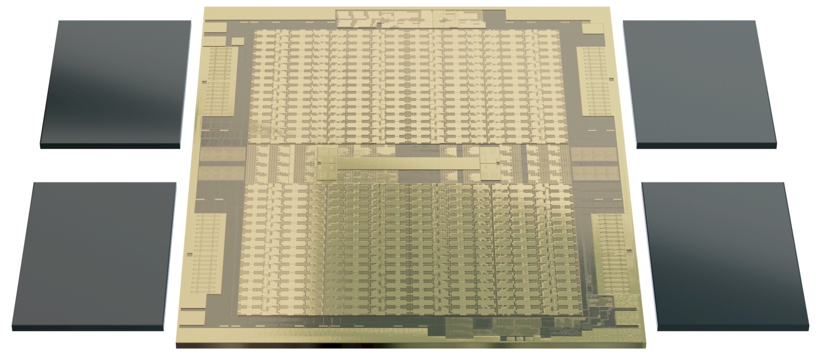
Here is what the Arcturus die looks like with its four banks of HBM2 memory visually aligned with it (but obviously not logically connected:
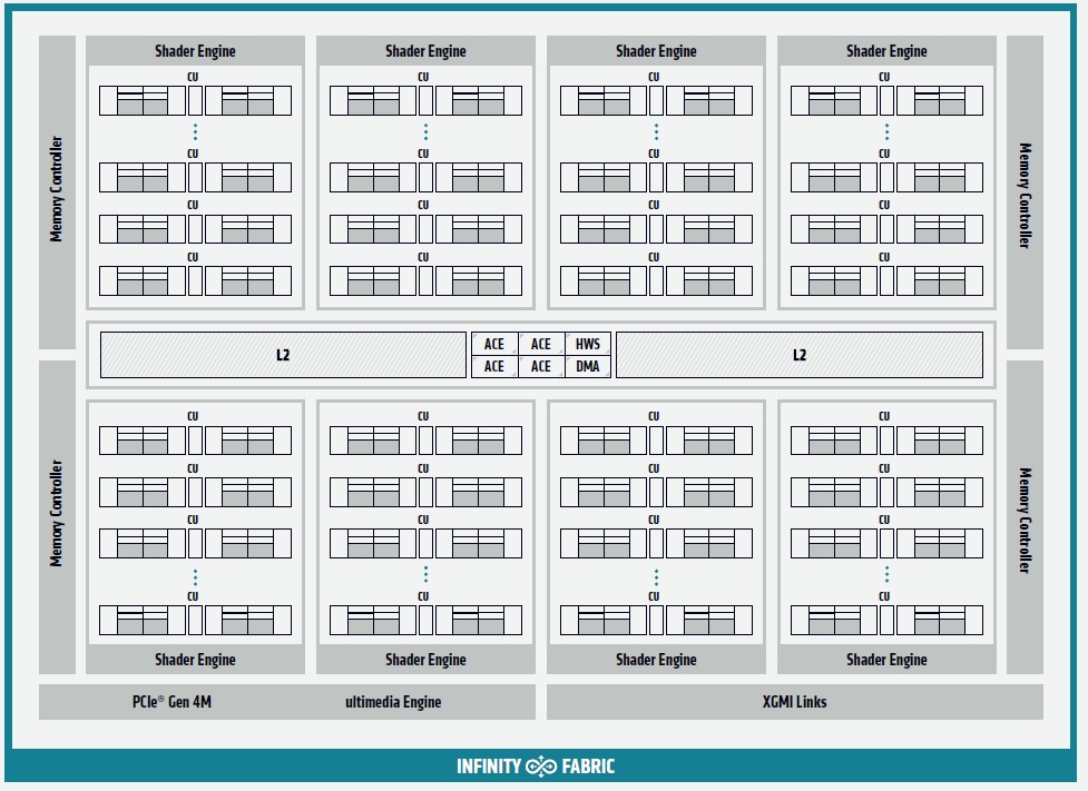
And here is the block diagram that shows what the elements of the Arcturus GPU are at a high level:
The compute elements are broken into eight banks, with two banks with a total of 32 compute elements sharing each HBM2 memory controller and therefore 8 GB of HBM2 memory. We strongly suspect that AMD will eventually double up the HBM2 memory on the Instinct MI100 accelerator cards at some point, particularly with Nvidia now boosting the HBM2 memory on its Ampere A100 card from 40 GB across five active controllers (the design has six, but one is latent) to 80 GB as part of its SC20 announcements today. The Arcturus memory controllers support HBM2 stacks that are four chips high or eight chips high, and we think the initial Instinct MI100 cards are using the four-high stacks at 2 GB per chip. If this is the case, then 64 GB is possible at some point in the future by stacking the memory twice as high. The current configuration has the memory supporting 2.4 GT/sec, delivering 1.23 TB/sec of aggregate memory bandwidth, which AMD says is 20 percent more bandwidth than with the Instinct MI50 card but in the same power envelope for the memory.
The Arcturus design has two blocks of compute engines, top and bottom, with two banks of 16-way associative L2 cache that has a total of 32 slices, linking them all to each other. The L2 cache capacity weighs in at a total of 8 MB and delivers an aggregate 6 TB/sec of bandwidth into and out of the compute engines. All of the memory has ECC error detection and correction, of course, which is necessary for compute workloads and less so for plain vanilla graphics, which can survive a bit error burp.
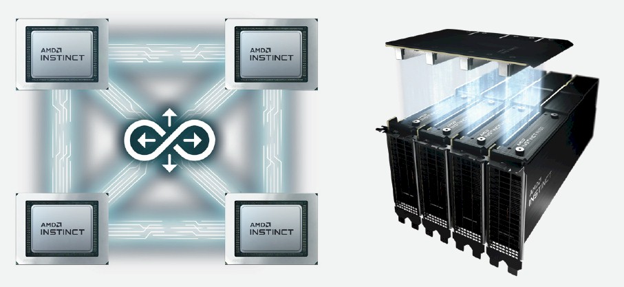
The whole shebang is wrapped up with AMD’s Infinity Fabric, a superset of the HyperTransport point-to-point link that was the heart and soul of the Opteron CPU architecture from more than a decade ago and that has been expanded and extended in many ways, including its use as a GPU-to-GPU interconnect and at some point in the future with CPU-to-GPU interconnect. The important thing is that Infinity Fabric supports coherent memory across devices, just like Nvidia’s NVLink does. On the Arcturus GPU compute engines, the Infinity Fabric runs at 23 GT/sec and is 16-bits wide, just like on the MI50 and MI60 Vega 20 GPUs, but with the Arcturus MI100 cards, there are three Infinity Fabric links coming off the die so that four GPUs can be crosslinked with only one hop between any two devices. Each one of those Infinity Fabric pipes has 92 GB/sec of bandwidth.
Having three Infinity Fabric pipes per Arcturus GPU allows a NUMA-like coupling of four GPUs and 128 GB of HBM2 memory into a much bigger virtual GPU, much like UltraPath Interconnect at Intel (a follow-on of QuickPath Interconnect, which is itself inspired by the Opteron design) allows for four CPUs to be tightly linked and share memory with only one hop in the “Cooper Lake” Xeon SP generation. Here is what an Infinity Fabric “hive” of four GPUs looks like:
With only two Infinity Fabric ports on the Instinct MI50 and MI60 cards, banks of GPUs could only be hooked to each other in a ring topology and the larger the number of GPUs in the ring, the more latency between the devices.
At some point in the future, the Epyc CPUs and the Instinct GPUs will have enough Infinity Fabric ports to cross couple a single CPU to a quad of GPUs, all with coherent memory across the devices. IBM has supported such coherence between Power9 processors and Nvidia V100 GPU accelerators for the past three years, and it is one reason that Big Blue won the contracts to build the “Summit” hybrid supercomputer at Oak Ridge National Laboratories and its companion “Sierra” supercomputer at Lawrence Livermore National Laboratories. For whatever reason, this coherence between CPU and GPU will not be available with the Power10 processors and the current Ampere GPUs and we presume future Nvidia GPUs because IBM wants to use OpenCAPI and Nvidia wants to use NVLink, and this may be one reason why Big Blue didn’t win the contracts for the follow-on “Frontier” and “El Capitan” exascale-class systems at these two labs in the United States. That said, the fallout over OpenCAPI and NVLink could be one result of losing the deal, not necessarily an effect.
At this point, the Instinct MI100 cards link to processors using standard PCI-Express 4.0 x16 links, which support 32 GB/sec of bandwidth in each direction, to and fro, between the devices. Add it all up, and each Instinct MI100 card has 64 GB/sec of PCI-Express 4.0 bandwidth and 276 GB/sec of Infinity Fabric bandwidth across its three pipes, for a total of 340 GB/sec of I/O bandwidth.
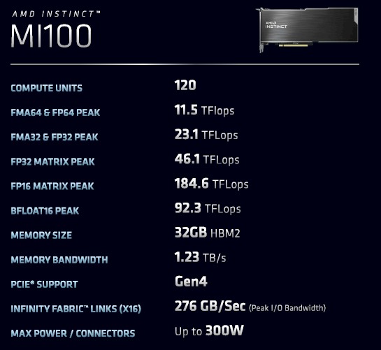
We will be doing a deep dive on the Arcturus GPU, including its new Matrix Core architecture and how it compares and contrasts with prior Instinct cards and Nvidia GPU compute engines, but for now, here are the raw feeds and speeds:
As you can see, only 120 of the 128 compute units on the Arcturus die, and therefore only 7,680 of its potential 8,192 streaming processors are activated. There is another 6.7 percent performance boost at the same clock speed inherent in the design as TSMC 7 nanometer yields improve – but as we say above, we wouldn’t count on it. The fun bit is that Arcturus is the first GPU accelerator to break through the 10 teraflops floating point barrier 64-bit precision – and AMD is doing it in a 300 watt thermal envelope for 11.5 teraflops, not a 400 watt one like Nvidia has with its Ampere A100, which weighs in at only 9.7 teraflops at 64-bit precision floating point. But, Nvidia has its own latent capacity in the Ampere device too. Who will get the TSMC yield up faster? Hmmmm. . . .
Pricing on the Instinct MI100 was buried in the footnotes, and is $6,400 a pop in single unit quantities. We are going to try to see what the OEMs are charging for it. Here are the initial OEM vendors and their machines that will support the MI100 GPU accelerator:
These OEMs will begin shipping these machines starting this month.




Puts on ai cloud based resulution 8k two minute papers on YouTube enhancers on gpu drivers and on gpu die and hardware after fixing the water cooling system for a thermo battery heat off loader system to the water battery pump from Intel like cyro cpu cooler.
“Infinity Fabric runs at 23 GT/sec”
what is limiting this to 23 GT/sec? Is it a GPU limit or a thermal limit?
That’s a good question but my guess is die area, power, and heat.
Which interconnect is faster? Amd Nvidia or Intel ?
NVLink supports 50 GT/s per lane.
GA100 supports 96 lanes (in+out) yielding 300 GB/s in and 300 GB/s out for a total bandwidth of 600 GB/s.
Nothing about the software side 🙁