There’s no resting on your laurels in the HPC world, no time to sit back and bask in a hard-won accomplishment that was years in the making. The ticker tape has only now been swept up in the wake of the long-awaited celebration last year of finally reaching the exascale computing level, with the Frontier supercomputer housed at the Oak Ridge National Labs breaking that barrier.
With that in the rear-view mirror, attention is turning to the next challenge: Zettascale computing, some 1,000 times faster than what Frontier is running. In the heady months after his heralded 2021 return to Intel as CEO, Pat Gelsinger made headlines by saying the giant chip maker was looking at 2027 to reach zettascale.
“So, zettascale in 2027 is a huge internal initiative that is going to bring many of our technologies together,” Gelsinger said in October 2021, responding to a question from The Next Platform. “1,000X in five years? That’s pretty phenomenal.”
Lisa Su, the chief executive officer who has led the remarkable turnaround at Intel’s chief rival AMD, took the stage at ISSCC 2023 to talk about zettascale computing, laying out a much more conservative – some would say reasonable – timeline.
Looking at supercomputer performance trends over the past two-plus decades and the ongoing innovation in computing – think advanced package technologies, CPUs and GPUs, chiplet architectures, the pace of AI adoption, among others – Su calculated that the industry could reach the zettabyte scale within the next 10 years or so.
“We just recently passed a very significant milestone last year, which was the first exascale supercomputer,” she said during her talk, noting that Frontier – built using HPE systems running on AMD chips – is “using a combination of CPUs and GPUs. Lots of technology in there. We were able to achieve an exascale of supercomputing, both from a performance standpoint and, more importantly, from an efficiency standpoint. Now we draw the line, assuming that [we can] keep that pace of innovation going. … That’s a challenge for all of us to think through. How might we achieve that?”
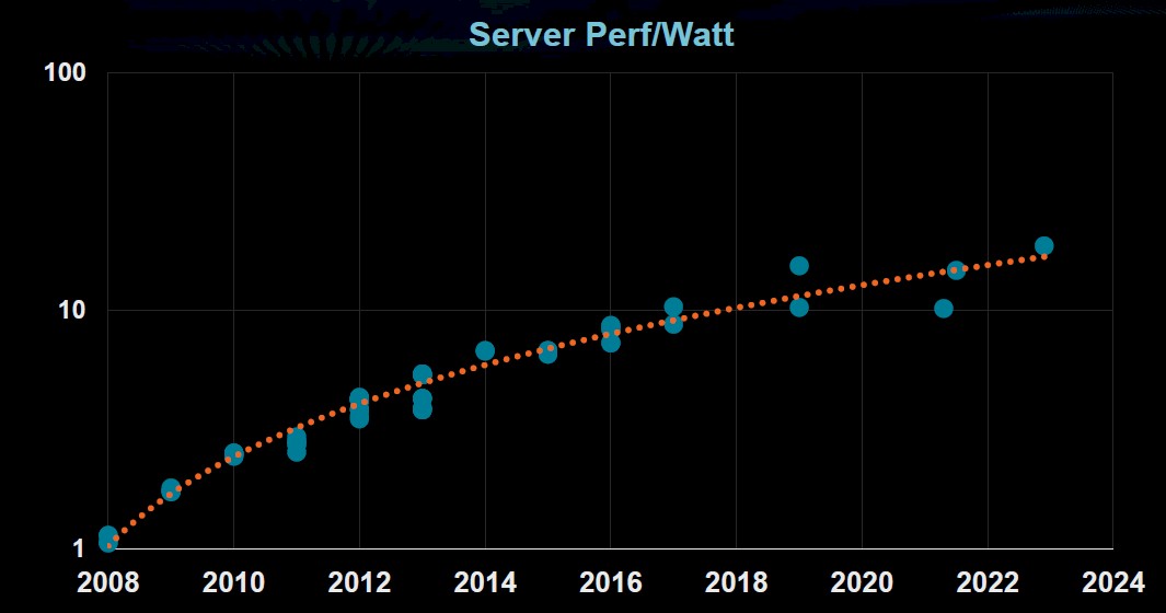
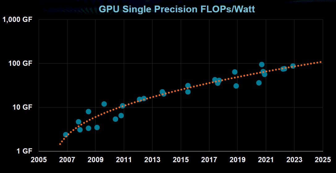
The crux of the challenge will be energy efficiency. While the performance of datacenter servers is doubling every 2.4 years, HPC computing every 1.2 years, and GPUs every 2.2 years, server efficiency is starting to flatten.
For GPUs, it is tailing off a bit as well:
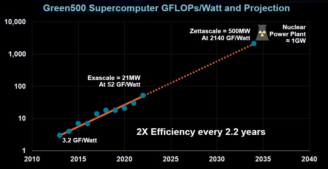
Meanwhile, supercomputing efficiency is doubling every 2.2 years, but that still projects to a zettascale system around 2035 consuming 500 megawatts at 2,140 gigaflops per watt.
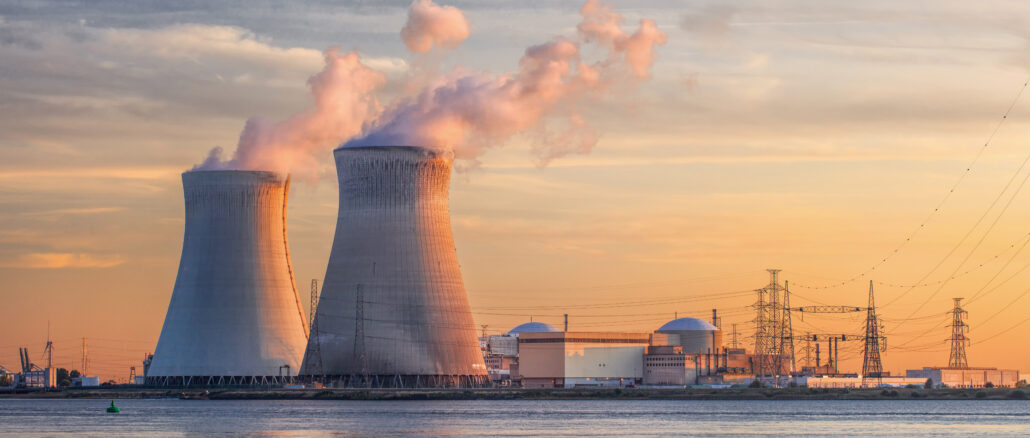
“It’s not practical for us to do that,” Su said. “It’s on the order of what a nuclear power plant would be, so this fundamentally says our challenge is to figure out how over the next decade we think about compute efficiency as the number-one priority. There’s a lot of work that has been done across the industry, but this is the number-one challenge that we have to continue the dramatic increases in performance and capability that we have seen.”
It’s doable. Along with being the world’s fastest computer – faster than the next six systems on the Top500 list combined – Frontier also came in second on the Green500 list of the world’s most efficient supercomputer.
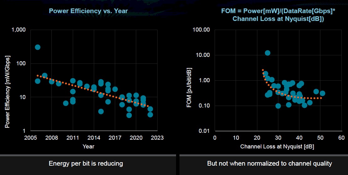
But there are challenges that make continued efficiency more difficult, including the slowing of Moore’s Law, making it more difficult to get both density performance and efficiency. Another is that IO doesn’t scale the way logic does. There have been gains in energy per bit, but in large part it’s because IO distances are getting smaller. However, in much larger systems like supercomputers, I/O continues to be a limiting efficiency factor. Here is a plot of the energy efficiency of I/O that Su presented:
Larger datasets and the bandwidth between compute and memory is eating up greater amounts of memory access power as well.
“What do we need to do over the next decade?” she asked. “It’s really driving system-level efficiency holistically, thinking about all of the elements across computation, across communications, and across memory that will enable us to achieve the most efficient systems.”
The area AMD focuses most on is in advanced architecture, with the goal of using “the right compute technology for the right workload,” Su said. “If you think about this whole conversation about heterogeneous architectures or accelerated computing, that’s really what we’re trying to do.”
Frontier uses AMD’s Instinct MI250 accelerator, a 6-nanometer GPU with more domain-specific architectural enhancements for HPC and AI workloads, more integration with chiplets, and a 2.5D chiplet integration, which brings high-bandwidth memory closer to the compute
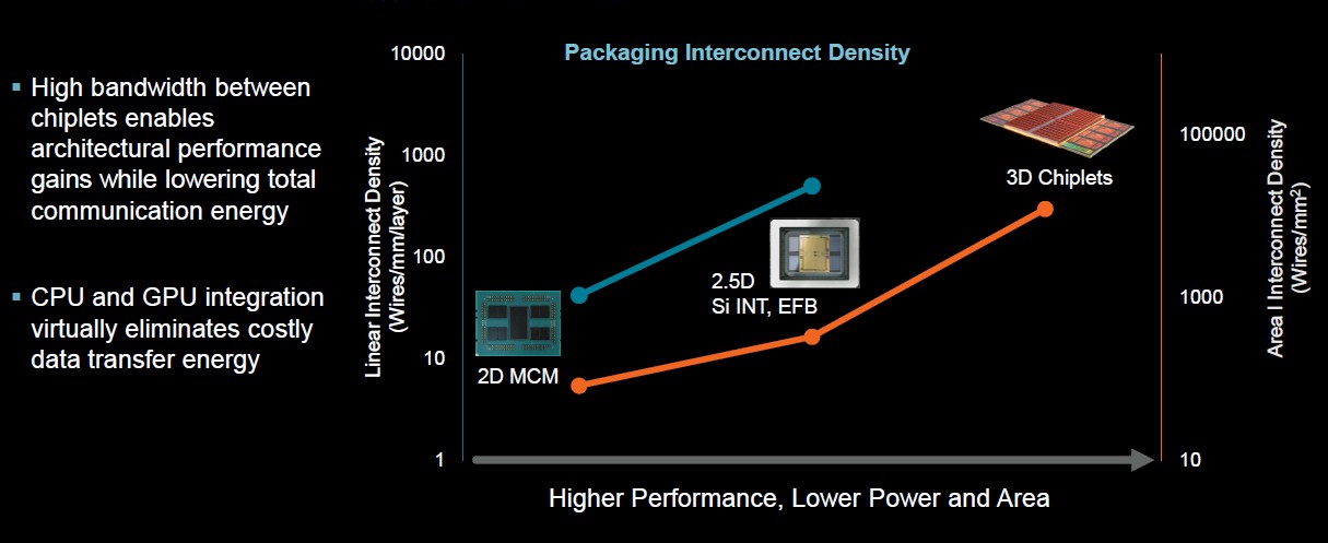
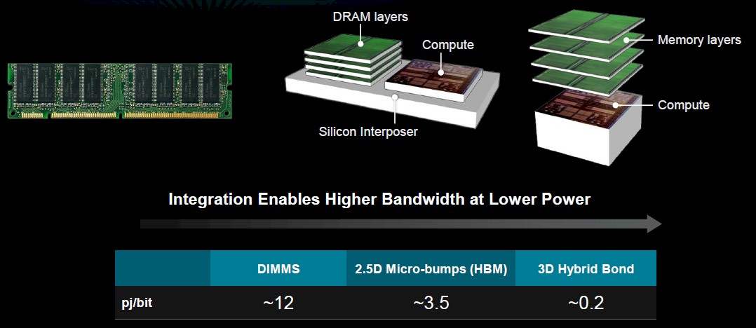
Now 3D chiplets are beginning ramp in the industry, and Su talked about the idea of stacking memory on top of the compute, reducing the amount of power needed for the processor to access memory.
“What it really does is it allows us to bring the components of compute much closer together and reduce the cost of communications,” the CEO said. “When you had these compute elements on a board – and how far [apart] they were and how much energy you had to spend communicating between them – now you can have them either on package in a 2D or 2.5D arrangement or stacked in a 3D arrangement and you see just a tremendous improvement in overall communication efficiency.”
Domain-specific computing is another area she pointed out, essentially using the right tool for the right operations. Moving from double-precision floating to point to other math formats means more efficient computing, particularly if AI and machine learning can be leveraged in the process to drive more automation. It also means more specific acceleration for particular applications.
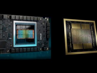
Pulling all this together results in the next-generation GPU, the Instinct MI300, which we talked about in-depth here last fall, for both HPC and AI workloads.
“With 5-nanometer process technology, with 3D stacking, with actually stacking our cache, fabric die on the bottom, stacking the CPUs and GPUs on top, with new math formats, with the different memory architecture, you can see improvements on the order of 5 to 8x, whether you’re talking about efficiency or whether you’re talking about performance,” Su said.
Stacking will be important with CPUs and GPUs, which typically have their own memory cache, which means having to move data around the processor if they want to share it. The MI300’s CDNA 3 APU architecture includes a unified memory architecture, making accessing the data more power efficient by eliminating the redundant memory copies needed in the MI250 and its separate memory caches.
Su touched on other innovations that need to come in such areas as memory and compute stacking.
“What we’ve demonstrated so far is SRAM stacking on compute die,” she said. “We put that into production and it has a significant improvement in certain workloads, not in all workloads. But there’s more opportunity here in terms of stacking DRAM on compute, stacking other types of memory.”
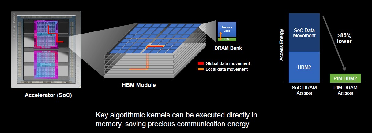
AMD also is working with Samsung around putting processing into memory, which Su admitted that, “as processor person, that seems that seems a little counterintuitive.” That said, there are some processing operations that likely can be inserted into memory. Research teams from AMD and Samsung found that putting some algorithmic kernels onto memory can reduce the overall access energy by as much as 85 percent.
“The work here is just only on the individual components, but it’s also how applications would use such technology,” she said. “This is an area where a lot of cross-functional learning would need to happen.”
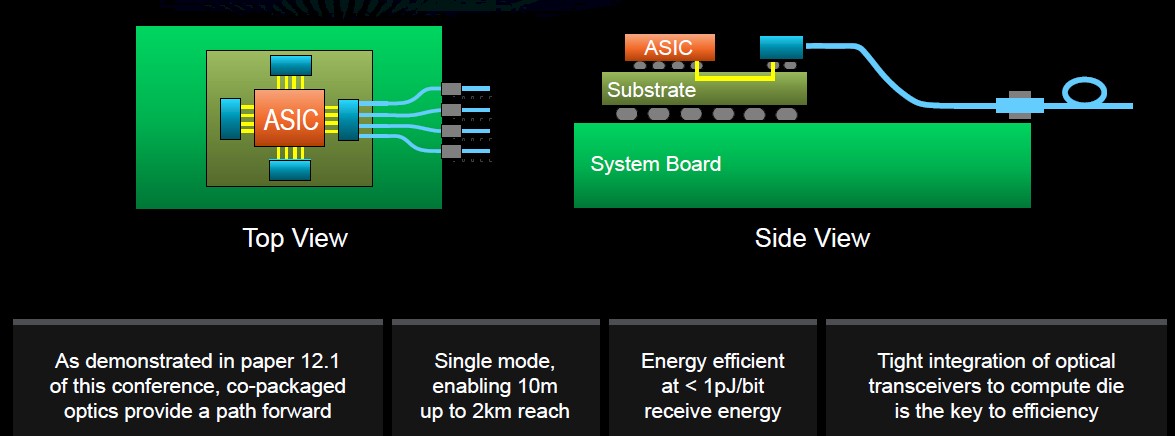
In addition, the chip maker is working with DARPA on co-packaging optical communications technologies to improve IO efficiency. Chiplet and condensed packaging is addressing local communication, but more needs to done to make longer-reach IO more efficient. One way would be tighter integration between the optical receivers and compute die in an optical setup.
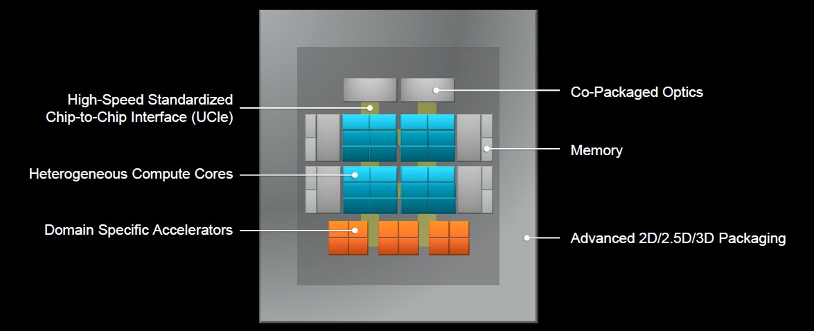
Eventually the goal is to get to a system-in-package architecture, with the package becoming the new motherboard, holding everything from CPUs and accelerators to memory and optics, Su said.
“That requires us to think differently on many levels,” she said. “From the compute standpoint, our goal would be to optimize every one of those compute cores to be the best they can possibly be. Whether it’s a CPU or a GPU or a domain-specific accelerator or whether you’re doing to an ASIC to do some machine learning – either training or inference – you can have each one of those compute cores to be optimized, but they should be able to be optimized by different people.”
Standardizing chip-to-chip interfaces becomes important to components can be mixed and matched.
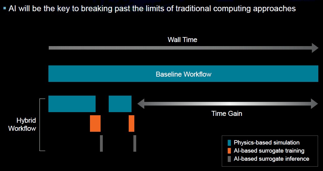
AI also will play an increasingly greater role in all this beyond being a tool for highly repetitive problems like training very large models. One area would be creating AI-surrogate physics models. For complex physics problems, the traditional solution is running CFD models using massive datasets.
However, AI-accelerated HPC “is the idea that you might do a part of the physics capability with traditional HPC computing and then you actually train on that data and then you can infer on that data so you can shorten the cycles,” Su said. “Then you might not be at the right answer yet, so you would go and train on a different set – presumably a smaller set – of the modeling. This is sort of a hybrid workflow.”
It’s still early and there is work that needs to be done to get the right algorithms and determining how to provision the problems, but it would mean bringing a more algorithmic thinking to system-level optimization. If the industry is going to improve power efficiency to the point of making zettascale computing a reality, these are the things that have to be done, she said.



co-packaged optics, 3d fabrication, standardized chip to chip interfaces, domain specific accelerators, silicon interposers … looks like Intel’s research projects from the last 15 years.
I question whether Zettascale is possible by the end of the decade if relying primarily on hardware advancements. I think Intel’s (R. Koduri’s) plan relies primarily on software advances and I vaguely recall Dr Su putting more emphasis on hardware/software co-optimization in her presentation.
Great summary of Su’s excellent ISSCC 2023 plenary talk (that kids can also watch on youtube, if so inclined)! The challenges we’re facing with energy dissipation come (I think) from our insufficient comprehension of the physics of matter (as a species). It would help, for example, if we could figure out room-temperature superconductivity, in a usable way. It would also be great if we could produce controllable electrical currents directly from nuclear processes (fusion, fission, or something other), rather than generating heat from them, using that heat to produce steam, using the steam to run a turbine, and then using the turbine to drive an electrical generator (alternator). Hopefully we can use Exascale (and beyond) computational tools to further our fundamental understanding of matter, and help us get to Zettascale (and beyond), energywise.
A problem with superconductor circuits is there are no efficient diodes.
… twistronics notwithstanding (magic-angle graphene …), or, hopefully, other superconducting switches with humorous, yet unanimously inspirational, names!
Chasing FLOPs is a stupid stunt. Go to the Top500 list and calculate efficiency. We already have way more FLOPs than we can use when the most computationally-dense benchmark gives us 60-65% efficiencies and something that looks like a real application (kind of) is at about 1%. Machines have been unbalanced for decades and FLOPs is a MEANINGLESS number.
So the supercomputers that will be sble to solve climate change will dissipate so much heat that they will fry the planet.
I sincerely hope the first one built is named “Malthus”!