
With the upcoming “Knights Landing” chip from Intel, the company is not only creating a follow-on motor for its Xeon Phi coprocessors, which are used as accelerators in conjunction with X86 processors inside servers. The company is also creating a standalone version that plugs into its own socket and is a compute engine in its own right. So it is perhaps only fitting that the Knights Landing processor – or rather a system that will eventually have that chip – was sighted at the Open Compute Summit in San Jose this week.
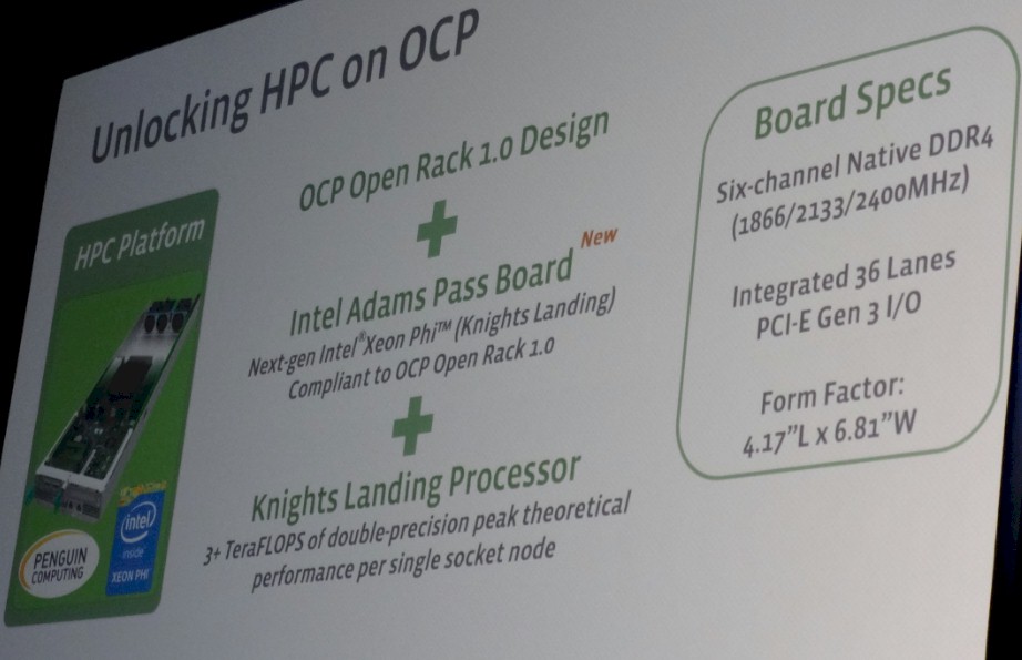
While talking about Intel’s various contributions to the Open Compute Project, the open source hardware effort that was started by Facebook and friends four years ago, Jason Waxman, general manager of the Cloud Platforms Group at Intel, flashed up this chart:
This is the first time that Intel has talked publicly about the motherboard it was designing for the Knights Landing processor, and it also mentions some feeds and speeds of the board (more on that in a minute) and that Intel is working with HPC specialist and Open Compute supplier Penguin Computing to deliver the first Open Compute node using the third generation Xeon Phi chip.
“There are a number of companies within the Open Compute community that want to do scientific research and high performance computing, but the form factors and the density can be quite challenging,” Waxman explained in his presentation. “We took that problem head on and we have worked with the community to take a new board – called Adams Pass, and this is a spec that we will also be opening up to the community – that will be a half width board supporting the next-generation Xeon Phi processor.” The Xeon Phi is expected in the second half of 2015 and is expected to have more than 60 of Intel’s “Silvermont” Atom cores, tweaked for HPC work, and delivering more than 3 teraflops of peak double precision floating point oomph. “You can actually get 10 gigaflops per watt out of this spec and motherboard design, and it is about 25 percent more efficient than an add-in card solution.”
This stands to reason, considering that you do not have to have a CPU in the mix running the applications along with the Xeon Phi – provided, of course, that the applications can be squeezed down to run on the cores in the Xeon Phi. Considering the very high compute capacity and memory bandwidth that the Knights Landing Xeon Phi processor will deliver, you can bet that more than a few companies doing modeling and simulation and other traditional HPC workloads will be looking at how they might adopt Knights Landing. You can also bet that any workload that would benefit from lots of threads and lots of memory bandwidth – data analytics in its myriad forms of streaming and static data – could also find a use with the Xeon Phi.
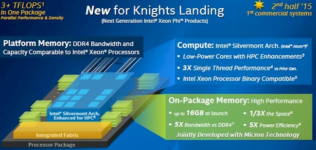
It is helpful to review what we know about the Knights Landing processor and then show how this chart tells us a little more about what is going on with the future Xeon Phi processor. Here is the chat Intel showed at last year’s ISC14 supercomputing conference:
The core used in the Knights Landing chip is a variant of the Silvermont core used in the “Avoton” C2000 series of Atom processors that were created by Intel to be used in system-on-chip designs aimed at server, storage, and network devices. Publicly, all that Intel has said is that the Knights Landing chip will have “more than 60 cores,” with the current “Knights Corner” Xeon Phi chip having a maximum of 61 modified Pentium 54C. The rumor mill has suggested that Intel can do as many as 72 cores on the Knights Landing die with the shrink to 14 nanometers, but Intel has never confirmed that. What is more important than the core count is that the chips will support 512-bit AVX math units and deliver three times the floating point performance as their Knights Corner predecessor.
A lot of that would seem to be coming from the “near memory” that Intel is welding onto the Knights Landing chip package. This memory is being created in conjunction with Intel partner Micron Technology, and it is based on the Hybrid Memory Cube (HMC) Gen2 stack memory that the two have been collaborating to create for several years. As the chart above shows, the HMC memory has five times the power efficiency as the GDDR5 graphics memory currently used on accelerators like the Xeon Phi coprocessors and GPU accelerators from Nvidia and AMD and five times the bandwidth of DDR4 memory used in the latest generations of Xeon servers. Intel plans to have up to 16 GB of this HMC near memory on the Knights Landing chip when it launches.
What Intel has not said is how much platform-level memory will be available as what it calls “far memory” in the Knights Landing systems that use it as a processor rather than a coprocessor linking into CPUs over a PCI-Express bus. All that the company has said is that it will use DDR4 memory and have bandwidth and capacity similar to that of its Xeon CPUs.
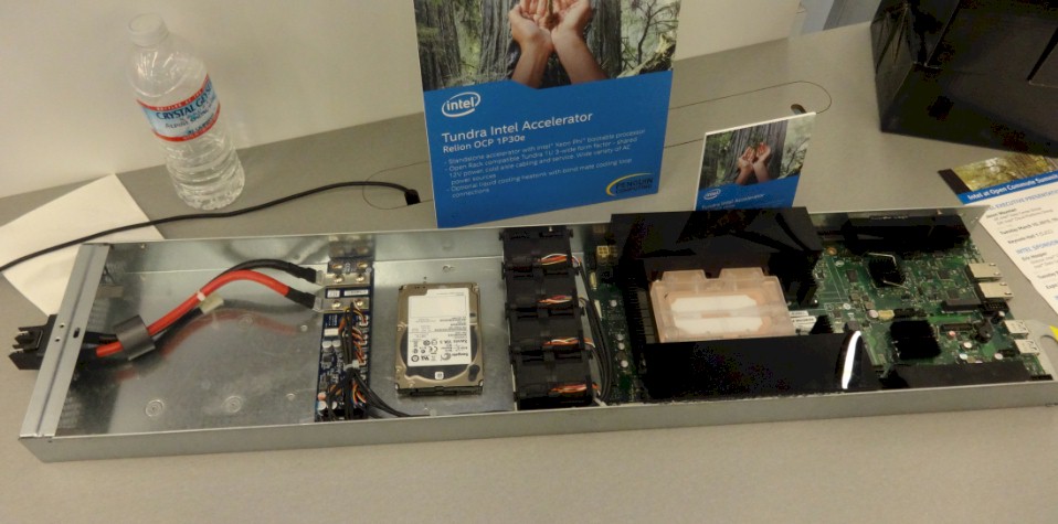
Indeed, we walked around the Open Compute Summit expo area, and found the Open Compute sled on display in the Intel booth, and the memory sockets on the Adams Pass board were covered over so no one could count them. Here’s the long shot of the Knights Landing sled:
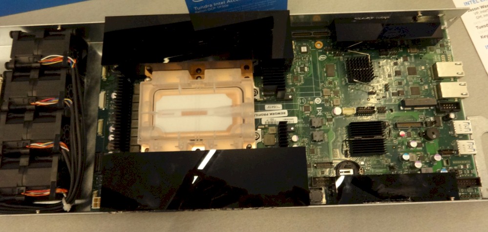
And here is a zoom in to show the board a little better:
But if you look back up at the slide that Waxman showed during his keynote, it says the Adams Pass motherboard into which the Knights Landing processor plugs has six-channel native DDR4 running at 1.87 GHz, 2.13 GHz, and 2.4 GHz speeds. There could be one or two memory sticks per channel. To my eye, the space on the left and right of the Knights Landing socket (if you are looking at the Open Compute sled from the front) had enough room for about six memory slots per side for a total of twelve. (That’s two DIMMs per channel.) But it is hard to say for sure. It might only be three slots on a side for a total of six. (One DIMM per channel.)
It is also interesting to see that the Adams Pass board will have 36 lanes of PCI-Express 3.0 I/O for its own peripherals. This will allow for the attachment of various networking and storage features, presumably. The hyperscale crowd likes Ethernet with an occasional detour into InfiniBand. Intel has said that it will integrate its next-generation Omni Scale fabric, a follow-on to InfiniBand, with the Xeon and Xeon Phi processors, but it is not clear if the Adams Pass board uses one of the Xeon Phi chips with on-die interconnect ports or one without. It would seem likely that for Open Compute customers, it would be without, given their overwhelming preference for Ethernet connectivity. Philip Pokorny, chief technology officer at Penguin, could not confirm or deny any of this, but he did tell The Next Platform that the future Tundra OpenHPC system that it had created using the Adams Pass board would support 81 nodes in an Open Compute rack. Fully loaded with compute, the Tundra rack has room for 96 nodes, and the remainder would be used up for switches, be they Omni Scale or InfiniBand for the typical HPC shop. The important thing is that Intel and Penguin can deliver over 243 teraflops in a rack, and at a power efficiency of 10 gigaflops per watt.
The other thing to consider is what applications could be ported to the Knights Landing chip to make use of something on the order of 5,700 cores that are compatible with the Haswell Xeon instruction set (minus the TSX transactional memory instructions). Datasets that fit inside of that 16 GB of near memory, and maybe even those that are cached in something on the order of 192 GB to 384 GB of DDR4 memory on the Adams Pass board, can be chewed on by the Knights Landing chip – whether or not you want to call it supercomputing.



Good job for getting this right:
[QUOTE]This memory is being created in conjunction with Intel partner Micron Technology, and it is based on the Hybrid Memory Cube (HMC) Gen2 stack memory that the two have been collaborating to create for several years. [/QUOTE]
But then … what happened here?
[QUOTE]As the chart above shows, the HMC memory has five times the power efficiency as the GDDR5 graphics memory currently used on accelerators like the Xeon Phi coprocessors and GPU accelerators from Nvidia and AMD and five times the bandwidth of DDR4 memory used in the latest generations of Xeon servers. Intel plans to have up to 16 GB of this HMC near memory on the Knights Landing chip when it launches.[/QUOTE]
HMC is a memory and interface standard owned by the HMC Consortium, not Micron, of which Intel is not a member and Intel seems not to be using. If Intel was using HMC why wouldn’t they call it HMC? And why do you call it HMC? It’s probably just a stack of DRAM with an Intel interface. Does that make it HMC? By that definition does JEDEC standard HBM also get to be called HMC?
Given this image
http://www.penguincomputing.com/wp-content/uploads/2014/08/tundra-openhpc-sled-500×400.jpg
I’d guess that there’s only space for three memory slots on each side for a total of six slots.
Robin
There are two variants of the sled motherboard, one that is wider and has more room than the other. I did not think to measure, but it could be more.