
The gap between processor architectures in the datacenter server and on the desktop or on our laps or now in our hands thanks to transistor shrinks over the past decade is getting bigger. The demands of the three radically different sets of workloads means that you can’t just prune a server processor to make something that is suitable for a client or conversely take a desktop or laptop chip and gussy it up with some extra memory and I/O to turn it into a server engine.
This is the main reason why Arm Holdings, the subsidiary of the Softbank conglomerate that controls the Arm processor architecture that dominates in smartphones and is trying to get a shoehorn into the datacenter door, is bifurcating its processor line. It also looks like, to us at least, that Arm wants to make it easier for server chip partners to put together a sophisticated and competitive design without having to invest tens of millions of dollars in unique intellectual property.
This hefty and continuous investment is why Calxeda went bankrupt, why Broadcom left and maybe Qualcomm will follow, why Samsung gave up before even talking publicly about its server chip efforts, why AMD just stopped talking about its Arm server efforts as its Epyc X86 server chips came out, why Applied Micro’s server chip business changed hands twice in a little more than a year and has been revamped as Ampere, and why Marvell’s Cavium unit is still pretty much the only Arm server chip game in town. Well, unless you include HiSilicon and Phytium, which have no hope outside of China’s sphere of influence. We do include the Bluefield processors from Mellanox Technologies (which came about after its acquisition of EZchip) in the hunt, by the way, and Amazon could still do something interesting with its Anapurna Labs homegrown Arm chips, such as letting others buy them.
Everyone looking for competition in the server processor market has been disappointed in how long it has taken Arm to take any meaningful share away from the mountain of Intel Xeons that are overwhelmingly chosen as the motors of modern data processing for the vast majority of workloads in the world.
At one time, Arm aspired to get 20 percent of worldwide server shipments by 2020, and then a year later, in a moment of exuberance, it upped the ante to 25 percent by 2021 (before Softbank bought it). Those optimistic share figures were probably based at least in part on the expectation that IBM’s Power8 and Power9 would not present much of a threat in the glass house to Intel Xeons (not a fair characterization, perhaps), that Intel would act precisely as it did in raising Xeon prices even as the performance improvement rate slowed, and that AMD would have issues getting its “Naples” Epyc processors to market – either because of design issues or fab partners or both.
All things considered, Naples looks like it accomplished the task of getting the conversation to switch to Epyc and away from the Arm collective at a lot of datacenters, thanks to the software compatibility that Epycs have with Xeons and the rough ride the Arm server chip makers have had. CIOs hate risk more than anything else. The market has expanded to give AMD perhaps 5 percent by year’s end and still not hurt Intel at all, because nobody ever got fired for buying Intel. (Not yet, anyway. They used to say that about IBM, remember?) And it looks like the new Neoverse line of infrastructure chips are being crafted by Arm to take away a little more risk than the prior generations of Cortex A series processors that were morphed into server engines did.
We have to infer that more than know that based on the relatively thin amount of information that Arm’s top brass are giving out at its TechCon conference in San Jose this week. But Drew Henry, senior vice president and general manager of the infrastructure line of business at Arm, gave us some hints and laid out the skeleton of the Neoverse plan.
The Changing Datacenter Changes Processing
Back in the heyday of Unix workstations and their emergence as server platforms, Henry was general manager of SGI’s visual computing business, and after playing around at some startups, did nearly eleven years at Nvidia running its GeForce graphics card business. After that, Henry did three years at SanDisk running its client platform flash business, selling to all of the hyperscalers and telcos for their various consumer devices, and then worked at some stealthy startups working on parallel computing and machine learning issues before taking the job at Arm in September 2017. We talked to Henry last November a few months after he settled in to the new job, and the Neoverse launch is the culmination of the work he has done for the past year to better align Arm with the future of the datacenter and the edge.
Like many, we have come around to the idea that a lot of computing will be done at the edge that might have otherwise been done in a datacenter. This is about dealing with data that is growing a lot faster than the Moore’s Law pace of days gone by at the same time that Moore’s Law is slowing down and so is the pace of capacity and price/performance increases in compute, networking, and storage. (Some clever engineering in signaling is saving networking in recent years, but 100 Gb/sec signaling lanes seem to be a pretty big barrier looking ahead.) Data will have to be chewed on at the edge because it is just too expensive and time consuming to move it back to a datacenter. We will be living in a world, perhaps, with no datacenter at all, but with a data and compute mesh – a data galaxy, perhaps – with escalating levels of consolidated and refined data and varying capacities of compute, storage, and networking to support that.
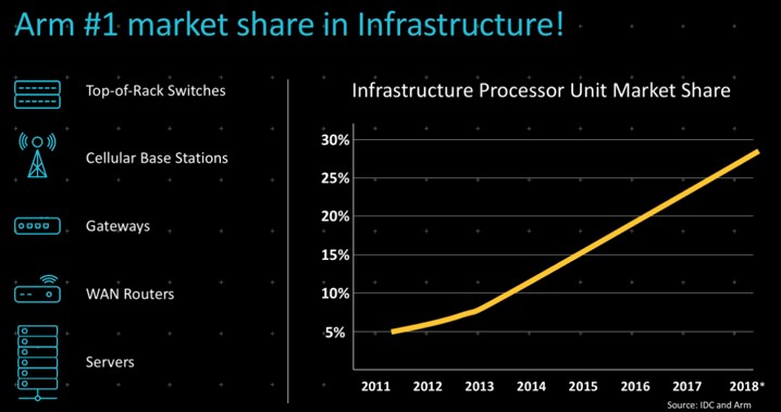
Before getting into the specifics of the Neoverse chip plan and roadmap, Henry did a recap to remind us that Arm has a very large presence in the datacenter today, even if the architecture’s share of traditional serving is small.
This means rolling in the share of chips that the Arm collective sells into cellular base stations as well as switches, gateways, WAN routers, and the smidgen of servers, and that share has grown from around 5 percent seven years ago to almost 30 percent so far in 2018.
With this presence in the datacenter and absolutely dominant share in smartphones, Arm has perhaps the best holistic view of how datacenters and devices are interacting and how this is changing. The model of cloudy datacenters creating and distributing media content in its various forms – and 75 percent of the capacity transmitted these days is video, although we would argue that the information content does not yet rival other traditional media such as text and voice – to billions of PCs and smartphones is evolving, according to Henry. Soon, it will be a collection of datacenters that work in conjunction with edge centers that feed into devices, with a lot more back and forth up and down the networks between them. Like this:
There will be three orders of magnitude increase in both datacenters – if you add up all of the edge centers, there will be tens millions of them – that will connect to three orders of magnitude more devices – tens of trillions of them. It will be a very chatty world, with much machine learning inference and data distillation and local reaction to raw, instantaneous, and ephemeral data. It will truly be an Internet.
“There is a redistribution in the way that processing is being done,” Henry explains. “Processing is moving from the core to out to the edge and even into devices themselves for applications that are latency intolerant. We are deeply involved in how these different systems are being devised.”
A New Turn
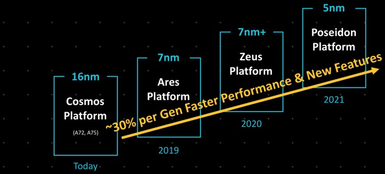
The Neoverse line of chips will draw on the current Cortex-A72 and Cortex-A75 designs, which will be recast with enhancements and made with tools and masks that are compatible with the current crop of 16 nanometer and 14 nanometer processes at Taiwan Semiconductor Manufacturing Corp as well as the equivalents at Samsung and GlobalFoundries – the three big independent fabs. Henry did not divulge what these chips, which he called a fork of the Cortex-A72 and Cortex-A75, would have that make them distinct, but we will find out soon enough. We do know that they will be recast as the “Cosmos” platform, and will be implemented in 16 nanometer processes, as the roadmap shows:
Next year, Arm will introduce the “Ares” successor to the Cosmos tweak, and this is where things get interesting. As the chart above suggests, Arm is promising an architecture that will deliver around 30 percent more performance with each generation, and an annual cadence to the designs that will keep the performance coming. By 2021, the chip designs that Arm will put out will, if this pace can be held, deliver 2.2X more performance. (By which Arm means aggregate compute throughput, not single thread performance, since clock speeds are going down as core counts go up.)
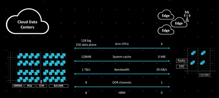
Arm did talk a bit about the Neoverse platform coming next year, which will be geared for heavy datacenter jobs like network function virtualization dataplanes and servers all the way down to edge devices with a modest number of cores, like this:
Neoverse means a new turn, and it means a new front in the war with Intel. And the Arm collective will be bringing to bear the 7 nanometer processes at TSMC and Samsung as well as whatever United Microelectronic Corp, the other Taiwanese foundry that also operates fabs in Singapore and China. Globalfoundries, which is the combination of the fabs from AMD and IBM, is not on this list because it spiked its 7 nanometer efforts in August and is hunkering down to try to make money on other kinds of chips using refined 14 nanometer tech.
The Neoverse war plan calls for server processors that will eventually scale up to 128 cores. Our guess is that Arm will use a multichip module approach that leverages the Cortex-A72 blocks to get 48 cores on a die at first, and then puts eight cores on a chiplet or chip block at first with “Ares” in 2019, then twelve cores per chunk with “Zeus” in 2020, and then sixteen with “Poseidon” in 2021, which also switches to 5 nanometer chip etching. Variants used in dataplane applications that have up to 256 cores eventually, which is interesting indeed.
Given this, we could see an Arm core architecture here that is similar to that of IBM with the “Nimbus” and “Cumulus” Power9 chip variants, which has what IBM calls modular execution slices that provide two threads each. This gives IBM the capability of making a 12-core chip with eight threads per core or a 24-core chip with four threads per core; it could even make a 48-core chip with two threads per core if it wanted to – all with essentially the same transistors with just a slight modification for how the slices are organized. This may, in fact, be how the same Neoverse Arm chip can do 64 cores in a server configuration and 128 cores in a dataplane configuration. We also assume that Arm will bite the bullet and add out of order execution to the cores, which up until now it has left to licensees to do.
A lot of the transistor budget of the Neoverse chips for servers is going for caches, which will weigh in at 128 MB across L3 and L2 caches at the top end. That 1 TB/sec cited in the chart above is the bandwidth of the 8×8 mesh that will link chip blocks together. This could be for monolithic designs or for chiplet designs. That figure is not a gauge of the interconnect that links all of the cores and I/O and memory together. That should be a lot more than 1 TB/sec. The 24-core Power9 chip weighs in at 7 TB/sec across all of these elements on the interconnect bus.
It is not clear what the memory bandwidth will be across eight channels of memory in the Neoverse designs, but it will probably be around 120 GB/sec, depending on the memory speeds of DDR4 supported; it will get a lot higher with DDR5 memory, and even more so if Arm embraces buffered DDR5 memory. The memory bandwidth for the HBM variant could be quite high. The NEC “Aurora” vector processor can do 1.2 TB/sec with six ranks of HBM2 memory, so eight ranks could be as high as 1.4 TB/sec.
The Neoverse server architecture will support native 100 Gb/sec Ethernet, PCI-Express (presumably the 4.0 flavor since 3.0, which runs at half the bandwidth, is getting a little old), and CCIX ports (presumably running at the same 25 Gb/sec per lane per direction as IBM’s Bluelink ports and NVLink ports on Power9) for tightly coupling non-volatile memory and accelerators. The CCIX protocol, which provides cache coherency across processors and accelerators, can ride on top of PCI-Express 4.0 as well, so that is useful.
For edge uses, the Neoverse architecture will scale down to four cores with no fat cache, one channel of DDR4 memory with 20 Gb/sec of bandwidth with one memory channel but will include integrated 10 Gb/sec Ethernet ports and 4G and 5G cellular radios.
We presume there will be variants in between these two extremes, and that is where we also assume Arm chip manufacturing licensees will be doing their differentiation.
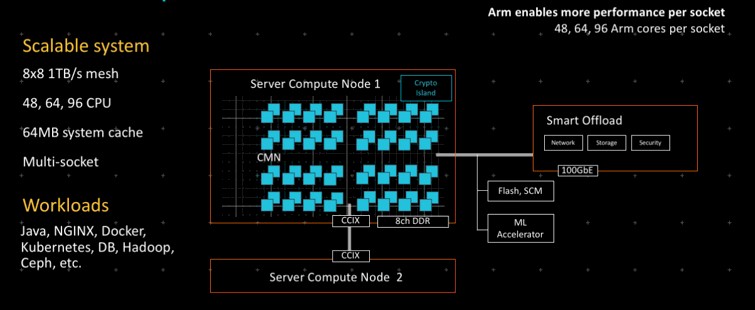
Henry unveiled more precise descriptions for how the Neoverse architecture will be used in various scenarios. Here is one for servers:
You can see how the core counts will scale up the Cosmos, Ares, and Zeus generations implied in the charts, with 64 MB of on-die cache, and how CCIX will be used to tightly couple servers. It is not clear if CCIX will be used to do NUMA interconnects, but given it is a cache coherent protocol and it is running at 25 Gb/sec, there is no reason why CCIX can’t be used in this fashion and also no reason why it could not, in theory, be used to make machines with two, four, or even eight sockets if there are enough CCIX ports on the chip to do topologies with relatively few hops. At some point, we think, the DDR memory channels will have to scale beyond eight, though, and that could happen with the top end Poseidon designs.
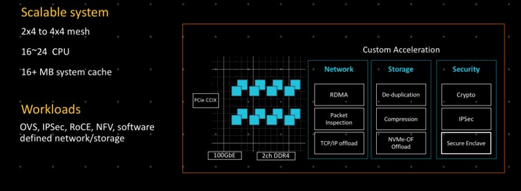
Here is how Neoverse will be tweaked to support network, storage, and security accelerators:
This architecture scales the interconnect mesh on the cores down to 2×4 and 2×4 mesh, with between 16 cores and 24 cores with somewhere around 16 MB of on-chip cache, with two channels of DDR memory and a more modest number of Ethernet, PCI-Express, and CCIX ports.
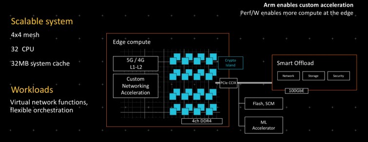
The Neoverse edge setups shoot the gap between these two:
It is basically half of a server processor with the 4G and 5G radios embedded, with the option of adding machine learning accelerators and offload engines for network, storage, and security over either PCI-Express or CCIX.
By the way, the Neoverse architecture has room to add on-die FPGAs, and that is probably good news for customers who like Xilinx malleable motors and want even tighter coupling than CCIX offers. (Xilinx is, of course, spearheading CCIX.)
Add it all up, and it could get quite a bit easier to field an Arm server chip, and there is more confidence in a long term roadmap that shows consistent performance growth, multiple fab partners, and a strong commitment to steady progress. This is how the Arm collective might attain that dream of 25 percent share in servers, commensurate with its existing share in other datacenter devices. Neoverse gives Arm much better odds.



Not sure what this throwaway sentence on out of order execution is on about – ARM licensed cores have been OoO since A9. This whole sentence on ARM doing something similar to Power’s core slice arch also makes very little logical sense; they’re almost certainly talking about different chip sizes and configurations.