

Computex, the annual conference in Taiwan to showcase the island nation’s vast technology business, has been transformed into what amounts to a half-time show for the datacenter IT year. And it is perhaps no accident that the CEOs of both Nvidia and AMD are of Taiwanese descent and in recent years have done the keynotes at Computex, usually unveiling new products or roadmaps.
The interesting twist is that AMD chief executive officer Lisa Su is a second cousin once removed to Nvidia co-founder and chief executive officer Jensen Huang, who gave his keynote on opening night for the Computex 2024 event in Taipei, unfolding the company’s compute and networking roadmaps between now and 2027. Su was the opening act on the first full day of the conference, and like Huang, she brought some silicon and some roadmaps.
Both Huang and Su are something akin to royalty in Taiwan, as you might expect.
Su got right down to business in her keynote, and spent a little more than half of her time talking about new Ryzen CPUs for PCs that are based on the Zen 5 cores and that are tuned up to accelerate AI workloads with neural network processors, or NNPs. While such matrix math units will likely eventually make their way into datacenter-class Epyc X86 CPUs, what we found interesting about the Ryzen discussion was the specs on the Zen 5 core that is at the heart of the current Ryzen 9000 series processors and that will be at the heart of the Turin Epyc servers CPUs that will launch in the second half of this year.
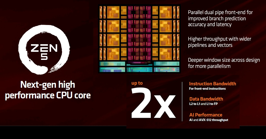
Su said that the Zen 5 core is the highest performing and most energy efficient core that AMD has ever designed, and that it was designed from the ground up.
“We have a new parallel dual pipeline front end. And what this does is it improves branch prediction accuracy and reduces latency,” Su explained. “It also enables us to deliver much more performance for every clock cycle. We also designed Zen five with a wider CPU engine instruction window to run more instructions in parallel for leadership compute throughput and efficiency. As a result, compared to Zen 4, we get double the instruction bandwidth, double the data bandwidth between the cache and floating point unit, and double the AI performance with full AVX 512 throughput.”
The top-end Ryzen 9000 has 16 cores and 32 threads and runs at 5.67 GHz turboed up, and the Zen 5 cores are averaging 16 percent more instructions per core than the Zen 4 cores used in prior Ryzen chips as well as in the “Genoa” Epyc 9000 series processors. (The “Bergamo” Epyc processors have more cores per socket with half the L3 cache per core and a different core layout called Zen 4c that allows greater core density.) The Zen 4 generation of Epycs have pushed up AMD’s share of the X86 server CPU space, and Su cited information from Mercury Research that showed AMD’s shipment share has grown from 2 percent in 2018 in the wake of the initial “Naples” Epyc 7001 series based, on Zen 1 cores, to 33 percent with the combination of Genoa Zen 4 cores and the Bergamo hyperscale and cloud CPUs and the “Siena” edge and telco processors based on Zen 4c cores.
Here is Su holding up the Turin Epyc package, which has 13 chiplets in total:

And here are the basic feeds and speeds for the Turin chips, also known as the 5th generation AMD Epyc:

We don’t really know much except that the top bin part will have 192 Zen 5 cores with 384 threads and will fit in the same SP5 sockets that the Genoa Epyc 9004s slip into. The Turin chips will likely be called the Epyc 9005s, and there will be variants that have a Zen 5c core that plug into the same machines that the Bergamo and Siena chips do today. We expect for something in the same ballpark for IPC as the Ryzen Zen 5 chips are seeing – call it somewhere between 15 percent and 20 percent IPC improvement over the Zen 4 cores.
Because Su is the sporting type, she came armed with some early benchmarks for the Turin chips.
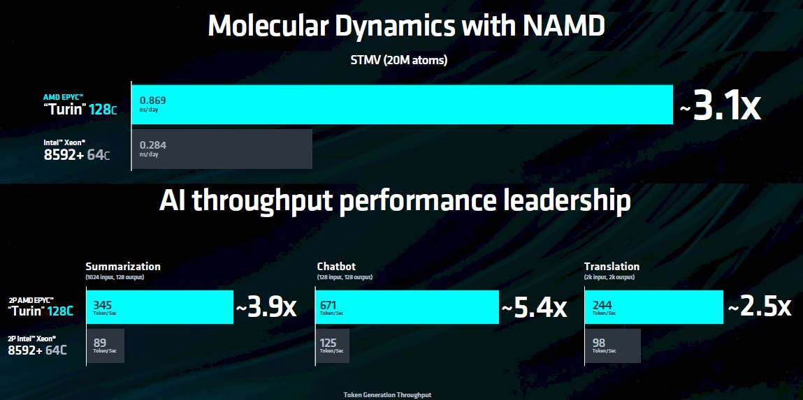
We consolidated two of the charts Su presented. At the top is the performance of a single Turin processor with 128 cores running the STMV benchmark in the NAMD molecular dynamics application. In this case, it is simulating 20 million atoms, and you count up how many nanoseconds of molecular interaction the compute engine can handle in a 24 hour day. (It is a bit curious why the 192 core chip was not tested here, but we assume it has another 33 percent higher performance on NAMD.) In any event, the 128 core Turin chip does about 3.1X the work of a 64 core “Emerald Rapids” Xeon SP-8592+ with 64 cores.
The AI throughput benchmarks are based on the Llama 2 model from Meta Platforms with 7 billion parameters and processing in INT4 data formats with inference token generation set at 50 milliseconds. The performance ranges between 2.5X and 5.4X depending on the workload.
That brings us to the Instinct GPU roadmap and performance comparisons of current and future AMD GPUs to current and future Nvidia GPUs.
Su went over the benchmarks first, and repeated that the “Antares” MI300 series was the fastest ramping product in AMD history, something she has said on calls with Wall Street and at other events recently. The reason is not just the availability of a GPU that at least looks and smells a bit like an Nvidia GPU in terms of the HPC and AI workloads it has been optimized to run, but also for the performance benefit and HBM memory capacity and bandwidth benefits that the AMD is offering over Nvidia.
Su said that for inference workloads, a server with eight MI300X GPUs had around 1.3X the performance of an Nvidia HGX board with eight H100 GPU accelerators running inference against the Llama 3 LLM with 70 billion parameters. On the Mistral 7B model, a single MI300X offered 1.2X the performance of an H100 GPU from Nvidia.
Looking into the future, Su showed another set of slides that said the CDNA 3 architecture in the MI300 series was around 8X faster at inference than the CDNA 2 architecture embodied in the “Aldebaran” Instinct MI200 series GPUs, but with an upcoming MI350 series GPU, the inference performance of the CDNA 4 architecture, which we think was pulled forward from the MI400 series expected next year, would increase inference performance by around 35X compared to the CDNA 3 architecture in the MI300.
Su then threw down the gauntlet and said that the MI350 would have 1.5X the memory capacity and 1.2X the AI compute power (as gauged by a blend of benchmarks using FP8, FP6, and FP4 performance) compared to Nvidia’s B200 GPU, expected in 2025 now as the Blackwell Ultra.
Without further ado, here is the updated AMD Instinct GPU roadmap:
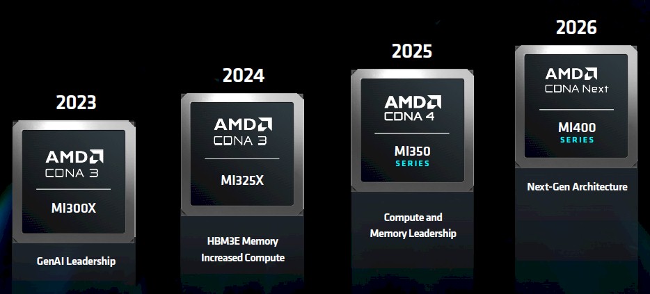
This year will see the addition of the MI325X, which will sport increased compute as well as a shift to HBM3E memory. Here are all the specs we know so far on this GPU:

How much more compute it will have remains to be seen, but the effective throughput of the device will likely double of the memory of the device goes up by 2X and the bandwidth goes up by 30 percent to 6 TB/sec on the HBM memory.
Here is how AMD is lining up the feeds and speeds of the MI325X to the Nvidia H200, which sports a 141 GB memory complex and that nearly doubles performance compared to the original H100 with 80 GB of capacity:
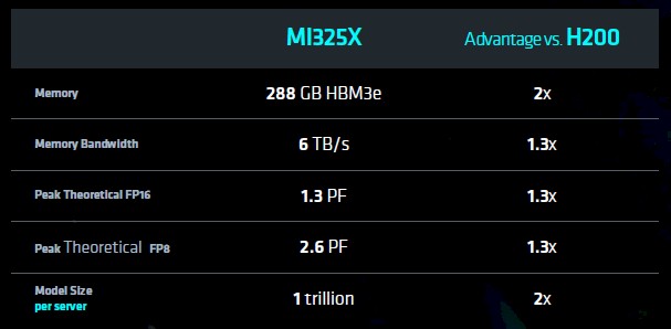
The important thing is that the parameters for a 1 trillion parameter model will fit into a system board with eight MI325X GPUs, with each GPU having 288 GB of HBM3E capacity.
The MI325X will be available in Q4 this year, and by that time, Nvidia will have some B100s in the field and will be shipping the H200s in full volume.
And that is why AMD moved up the CDNA 4 architecture and is putting out an MI350X, based on 3 nanometer processes from Taiwan Semiconductor Manufacturing Co and sporting 288 GB of HBM3E memory as well as FP6 and FP4 data types.

There could be an MI350A as well, and possibly other variations on the MI350 theme since AMD calls the MI350X “the first product in the AMD Instinct MI350 series.” The memory capacity and type is the same in the MI325X and the MI350X, and the difference might be that the HBM3E running in the MI350X might be cycling faster and therefore yielding a bit more bandwidth; 7.2 TB/sec would not surprise us.
You might be wondering why the MI350X won’t be using HBM4 memory when it ships in 2025. Nvidia is not expected to add HBM4 memory until it ships the “Rubin” GPUs in 2026, as we reported elsewhere. We do expect that the MI400 series that debuts in first products with the “CDNA Next” architecture in 2026 will use HBM4 memory.
All we know for sure is that the rush to improve inference performance next year moved the CDNA 4 architecture into the MI350 and broke the symmetry between Instinct GPU generations and their CDNA architecture level. We are almost halfway through 2024, so that means that whatever is in the CDNA 4.5 or CDNA 5 architecture expected to be used in the MI400 series has to be pretty close to being finalized right now.
AMD beating Intel in server CPUs was inevitable as the latter had foundry follies that — how to say this politely? — totally screwed up its product roadmaps. Catching up to and keeping pace with Nvidia in server GPUs is another thing entirely – and AMD has definitely done that and will be keeping pace for years to come. If AMD could clone Nvidia GPUs bug for bug and run its HPC and AI software stacks unchanged, as it does Windows and Linux workloads on Intel CPUs, it would be eating half of Nvidia’s enormous lunch. Provided it could get packaging and HBM memory, of course.

The Increasingly Graphic Nature Of Intel Datacenter Compute
When you get to the place where Intel is at in datacenter compute, you cannot dictate terms to customers. You have to listen very carefully and deliver what customers need or one of myriad different competitors will steal your milk money, eat your lunch, and send you to bed without …

AI Is Coming In The Front Door To Get The Back Office
Large language models can be fun, as shown by the wild popularity of ChatGPT since OpenAI tossed the generative AI chatbot into the public sphere in late November and let people have at it. According to a study by UBS, ChatGPT racked up more than 100 million active users in …
With AI, You Need To See The Bigger Hardware And Software Picture
Sponsored Feature: It’s a decade and a half since researchers dazzled the tech world by demonstrating that GPUs could be used to dramatically accelerate key AI operations. That realization continues to grip the imagination of enterprises. IDC has reported that when it comes to infrastructure, GPU accelerated compute and HPC …
“Catching up to and keeping pace with Nvidia in server GPUs is another thing entirely – and AMD has definitely done that and will be keeping pace for years to come”
How about asking for benchmarks between MI300 and H100 to start with? and, then make all the claims for future?
Server and workstation component Market Share in time period that is December 2023 through May 2024.
AMD B+G+S+TR7 = 46.62%
Intel ER+SR+Atoms+RaptorE = 54.38%
AMD adds Milan+TR5 = 29.93%
Intel adds Ice+RocketE = 70.07%
AMD adds Rome+TR3 = 14.72%
Intel adds Cascades+Coffee Refresh E = 85.28%
AMD adds Naples+TR2+TR1 7.78%
Intel adds Skylake+CoffeeE = 92.22%
AMD aforementioned = 3.26%
Intel adds BW+HW+Ivy = 96.73%
To calculate cores share, to see current server SKU supply, trade-in and sales trend across 817 individual Epyc, Threadripper and Xeon server and workstation SKUs, to compare AMD and Intel directly competitive SKUs that takes a bit more work on channel supply data dropped into your own Excell file see Server Today and lift the data from the first table down;
https://seekingalpha.com/instablog/5030701-mike-bruzzone/5509267-server-today
On AMD Instinct accelerators, very few as in count the number on your fingers escape their commercial use base. Under AMD license provision? While Mi125 is readably available from open market sources Mi2x0 and M13x0_ are not. Certainly not as many as Nvidia Blackwell, Hopper and Ampere. If AMD accelerators were more readily available in the broker market and usually begins with academic use subject learning, perhaps AMD accelerators would be better understood. Then again that may not be what Instinct end customers want on their own application development tools and keeping uses proprietary to themselves. mb
Pretty neat stuff. Some competition in the stratosphere. Now, will we ever see CDNA come back to us mortals in the small ISV space? AWS will rent me a VM with nV HPUs but not Mi300. Azure and Oracle claim to offer Mi300 but darned if I can find a way to provision such a VM. AMD should sell PCIe (a) cards with CDNA3/4 chips. It does not have to be a 1300 TF16 monster, 650 is fine. AI bubble is going to pop one day and when that happens AMD risks facing it’s old conundrum: all the software is written for CUDA. Few in the ISV world can afford the price of an 8 way MI300 machine… we need a reprise of the Radeon VII.